MK1725 データシートの表示(PDF) - Integrated Circuit Systems
部品番号
コンポーネント説明
一致するリスト
MK1725 Datasheet PDF : 6 Pages
| |||
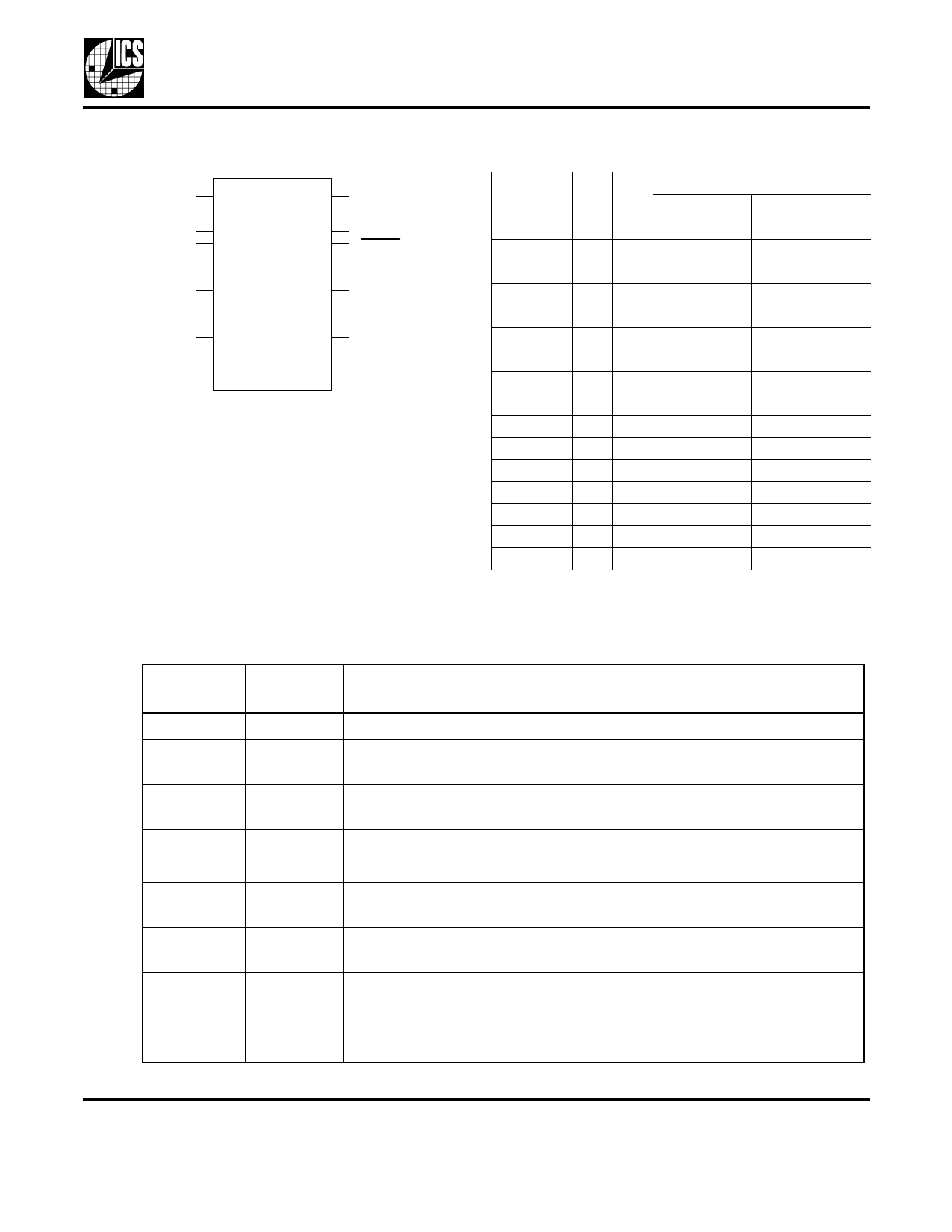
Pin Assignment
X1 1
S0 2
S3 3
VDD 4
GND 5
S1 6
CLK1 7
CLK2 8
16 X2
15 VDD
14 PDTS
13 S2
12 VDD
11 GND
10 CLK4
9 CLK3
16 pin (173 mil) TSSOP
MK1725
Quad Output Spread Spectrum Clock Generator
CLK Output Selection Table
S3 S2 S1 S0
0000
0010
0001
0011
0110
0101
0100
0111
1000
1010
1001
1011
1110
1101
1100
1111
CLK1:4
Multiplier
Spread %
1
-1%
1
-0.5%
1
+/- 0.5%
1
+/- 0.25%
2
-1%
2
-0.5%
2
+/- 0.5%
2
+/- 0.25%
4
-1%
4
-0.5%
4
+/- 0.5%
4
+/- 0.25%
1
OFF
2
OFF
4
OFF
TEST
TEST
Pin Descriptions
Pin
Number
1
2
Pin
Name
X1
S0
3
S3
4
VDD
5
GND
6
S1
7
CLK1
8
CLK2
9
CLK3
Pin
Type
Pin Description
Input Connect to a 20 - 34 MHz crystal or clock input.
Input Select pin 0. Determines frequency and spread amount on
output clocks as per table above. Internal pull-down.
Input Select pin 3. Determines frequency and spread amount on
output clocks as per table above. Internal pull-down.
Power Connect to +3.3V.
Power Connect to ground.
Input Select pin 1. Determines frequency and spread amount on
output clocks as per table above. Internal pull-down.
Output Clock 1 output. Frequency and spread amount are determined
by table above. Weak internal pull-down when tri-state.
Output Clock 2 output. Frequency and spread amount are determined
by table above. Weak internal pull-down when tri-state.
Output Clock 3 output. Frequency and spread amount are determined
by table above. Weak internal pull-down when tri-state.
MDS 1725 C
2
Revision 021605
Integrated Circuit Systems ● 525 Race Street, San Jose, CA 95126 ● tel (408) 297-1201 ●www.icst.com
Share Link: 