MIC5237(2000) データシートの表示(PDF) - Micrel
部品番号
コンポーネント説明
一致するリスト
MIC5237 Datasheet PDF : 8 Pages
| |||
MIC5237
Micrel
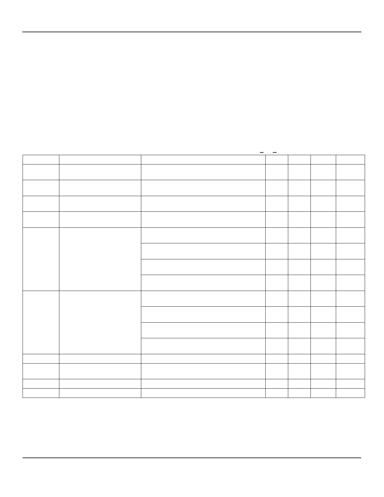
Electrical Characteristics
VIN = VOUT + 1.0V; COUT = 4.7µF, IOUT = 100µA; TJ = 25°C, bold values indicate –40°C ≤ TJ ≤ +125°C; unless noted.
Symbol
Parameter
Conditions
Min Typical Max
Units
VOUT
Output Voltage Accuracy
variation from nominal VOUT
–3
3
%
–5
5
%
∆VOUT/∆T
Output Voltage
Temperature Coefficient
Note 2
40
ppm/°C
∆VOUT/VOUT Line Regulation
VIN = VOUT + 1V to 16V
0.05 %/V
0.015 0.1 %/V
∆VOUT/VOUT Load Regulation
IOUT = 100µA to 500mA, Note 3
0.05 0.5
%
0.7
%
VIN – VOUT Dropout Voltage, Note 4
IOUT = 100µA
10
70
mV
90
mV
IOUT = 50mA
115 190 mV
280 mV
IOUT = 150mA
165 350 mV
450 mV
IOUT = 500mA
300 600 mV
700 mV
IGND
Ground Pin Current, Note 5
IOUT = 100µA
IOUT = 50mA
80
130
µA
170
µA
350 650
µA
900
µA
IOUT = 150mA
1.8
2.5
mA
3.0
mA
IOUT = 500mA
8
15
mA
20
mA
PSRR
Ripple Rejection
f = 120Hz
75
dB
ILIMIT
Current Limit
VOUT = 0V
700 900 mA
1000
∆VOUT/∆PD
eno
Thermal Regulation
Output Noise
Note 6
VOUT = 5.0V, IOUT = 50mA,
COUT = 2.2µF
0.05
500
%/W
nV/ Hz
Note 1:
Note 2:
Note 3:
Note 4:
Note 5:
Note 6:
Absolute maximum ratings indicate limits beyond which damage to the component may occur. Electrical specifications do not apply when
operating the device outside of its operating ratings. The maximum allowable power dissipation is a function of the maximum junction
temperature, TJ(max), the junction-to-ambient thermal resistance, θJA, and the ambient temperature, TA. The maximum allowable power
dissipation at any ambient temperature is calculated using: PD(max) = (TJ(max) – TA) ÷ θJA. Exceeding the maximum allowable power dissipa-
tion will result in excessive die temperature, and the regulator will go into thermal shutdown. See the “Thermal Considerations” section for
details.
Output voltage temperature coefficient is defined as the worst case voltage change divided by the total temperature range.
Regulation is measured at constant junction temperature using low duty cycle pulse testing. Parts are tested for load regulation in the load
range from 100µA to 500mA. Changes in output voltage due to heating effects are covered by the thermal regulation specification.
Dropout voltage is defined as the input to output differential at which the output voltage drops 2% below its nominal value measured at 1V
differential.
Ground pin current is the regulator quiescent current plus pass transistor base current. The total current drawn from the supply is the sum of
the load current plus the ground pin current.
Thermal regulation is defined as the change in output voltage at a time “t” after a change in power dissipation is applied, excluding load or line
regulation effects. Specifications are for a 500mA load pulse at VIN = 16V for t = 10ms.
January 2000
3
MIC5237
Share Link: 