MCP2140A データシートの表示(PDF) - Microchip Technology
部品番号
コンポーネント説明
一致するリスト
MCP2140A
Microchip Technology

MCP2140A Datasheet PDF : 60 Pages
| |||
MCP2140A
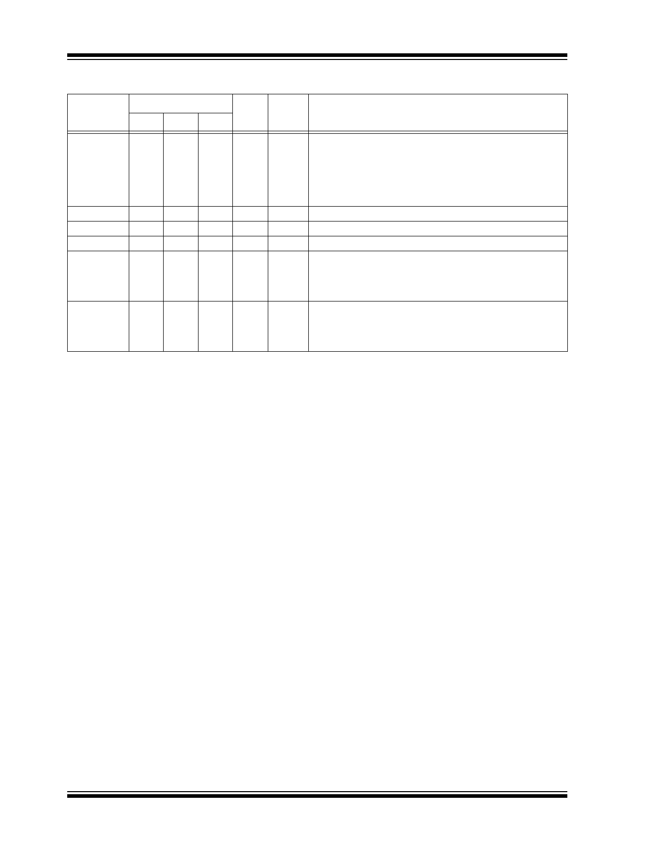
TABLE 1-1: MCP2140A PIN DESCRIPTION NORMAL OPERATION (DCE) (CONTINUED)
Pin Name
Pin Number
Pin
PDIP SOIC SSOP Type
Buffer
Type
Description
RTS
13 13 14
I
TTL Request to Send. Indicates that a Host Controller is ready to
receive data from the MCP2140A. This signal is locally
emulated and not related to the CTS/RTS bit of the IrDA
Primary device.
1 = Host Controller not ready to receive data
0 = Host Controller ready to receive data
VDD
14 14 15, 16 —
P Positive supply for logic and I/O pins.
OSC2
15 15 17
O
— Oscillator crystal output.
OSC1/CLKIN 16 16 18
I CMOS Oscillator crystal input/external clock source input.
CD
17 17 19
I
ST Carrier Detect. The state of this bit is communicated to the
IrDA Primary device via the IrDA CD bit.
1 = No Carrier Present
0 = Carrier Present
RXPD
18 18 20
I
A IR RX Photo Detect Diode input. This input signal is required
to be a pulse to indicate an IR bit. When the amplitude of the
signal crosses the amplitude threshold set by the RXPDREF
pin, the IR bit is detected.
Legend:
TTL = TTL compatible input
A = Analog
CMOS = CMOS compatible input
I = Input
ST = Schmitt Trigger input with CMOS levels
P = Power
OC = Open collector output
O = Output
Note 1: The state of the DSR output pin does not reflect the state of the DTR bit of the IrDA Primary Device.
DS22050A-page 6
© 2007 Microchip Technology Inc.
Share Link: