MC100E151FN データシートの表示(PDF) - ON Semiconductor
部品番号
コンポーネント説明
一致するリスト
MC100E151FN Datasheet PDF : 8 Pages
| |||
MC10E151, MC100E151
5V ECL 6-Bit D Register
Description
The MC10E/100E151 contains 6 D-type, edge-triggered,
master-slave flip-flops with differential outputs. Data enters the
master when both CLK1 and CLK2 are LOW, and is transferred to the
slave when CLK1 or CLK2 (or both) go HIGH. The asynchronous
Master Reset (MR) makes all Q outputs go LOW.
The 100 Series contains temperature compensation.
Features
• 1100 MHz Min. Toggle Frequency
• Differential Outputs
• Asynchronous Master Reset
• Dual Clocks
• PECL Mode Operating Range: VCC = 4.2 V to 5.7 V
with VEE = 0 V
• NECL Mode Operating Range: VCC = 0 V
with VEE = −4.2 V to −5.7 V
• Internal Input 50 kW Pulldown Resistors
• ESD Protection: Human Body Model; > 2 kV,
Machine Model; > 200 V
• Meets or Exceeds JEDEC Standard EIA/JESD78 IC Latchup Test
• Moisture Sensitivity Level:
Pb = 1
Pb−Free = 3
For Additional Information, see Application Note AND8003/D
• Flammability Rating: UL 94 V−0 @ 0.125 in,
Oxygen Index: 28 to 34
• Transistor Count = 304 devices
• Pb−Free Packages are Available*
http://onsemi.com
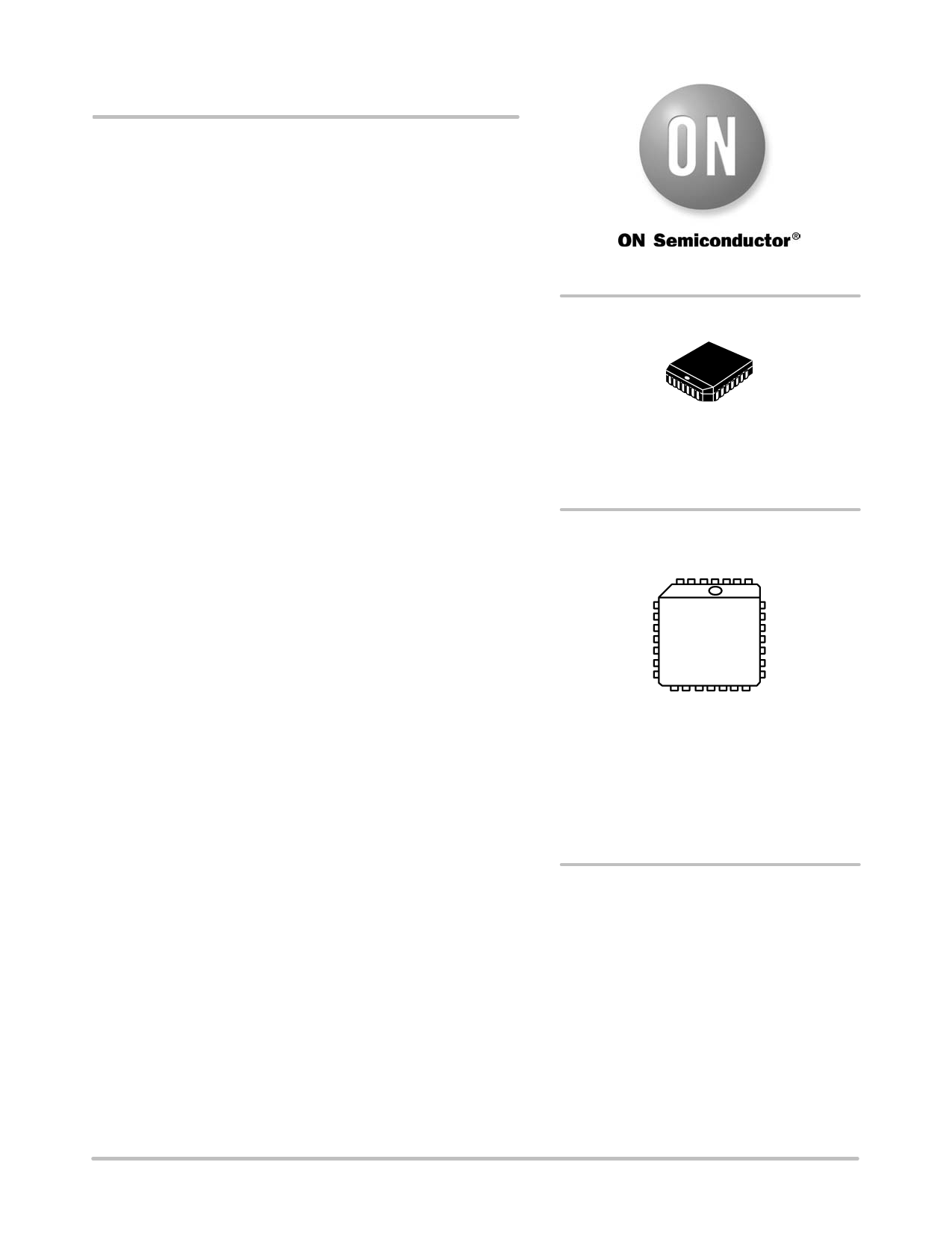
PLCC−28
FN SUFFIX
CASE 776
MARKING DIAGRAM*
1
MCxxxE151FNG
AWLYYWW
xxx
= 10 or 100
A
= Assembly Location
WL
= Wafer Lot
YY
= Year
WW = Work Week
G
= Pb−Free Package
*For additional marking information, refer to
Application Note AND8002/D.
ORDERING INFORMATION
See detailed ordering and shipping information in the package
dimensions section on page 6 of this data sheet.
*For additional information on our Pb−Free strategy and soldering details, please
download the ON Semiconductor Soldering and Mounting Techniques
Reference Manual, SOLDERRM/D.
© Semiconductor Components Industries, LLC, 2006
1
November, 2006 − Rev. 9
Publication Order Number:
MC10E151/D
Share Link: 