MC74HCT08A(2014) データシートの表示(PDF) - ON Semiconductor
部品番号
コンポーネント説明
一致するリスト
MC74HCT08A Datasheet PDF : 6 Pages
| |||
MC74HCT08A
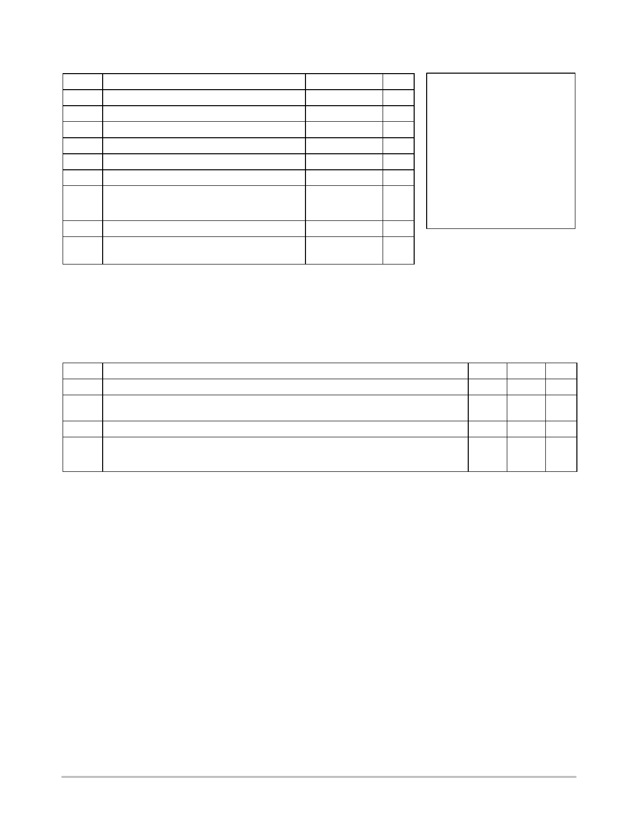
MAXIMUM RATINGS
Symbol
Parameter
Value
Unit
VCC DC Supply Voltage (Referenced to GND)
−0.5 to +7.0
V
Vin DC Input Voltage (Referenced to GND)
−0.5 to VCC +0.5
V
Vout DC Output Voltage (Referenced to GND)
−0.5 to VCC +0.5
V
Iin
DC Input Current, per Pin
±20
mA
Iout DC Output Current, per Pin
±25
mA
ICC DC Supply Current, VCC and GND Pins
±50
mA
PD
Power Dissipation in Still Air,
SOIC Package†
500
mW
TSSOP Package†
450
Tstg Storage Temperature
−65 to +150
°C
TL
Lead Temperature, 1 mm from Case for 10 Seconds
°C
SOIC or TSSOP Package
260
Stresses exceeding those listed in the Maximum Ratings table may damage the device. If any of
these limits are exceeded, device functionality should not be assumed, damage may occur and
reliability may be affected.
†Derating − SOIC Package: − 7 mW/°C from 65°C to 125°C
TSSOP Package: − 6.1 mW/°C from 65°C to 125°C
RECOMMENDED OPERATING CONDITIONS
Symbol
Parameter
VCC
Vin, Vout
DC Supply Voltage (Referenced to GND)
DC Input Voltage, Output Voltage
(Referenced to GND)
TA
Operating Temperature, All Package Types
tr, tf Input Rise and Fall Time
(Figure 3)
VCC = 2.0 V
VCC = 4.5 V
VCC = 6.0 V
This device contains protection
circuitry to guard against damage
due to high static voltages or electric
fields. However, precautions must
be taken to avoid applications of any
voltage higher than maximum rated
voltages to this high−impedance cir-
cuit. For proper operation, Vin and
Vout should be constrained to the
range GND v (Vin or Vout) v VCC.
Unused inputs must always be
tied to an appropriate logic voltage
level (e.g., either GND or VCC).
Unused outputs must be left open.
Min
Max Unit
2.0
6.0
V
0
VCC
V
−55
+125 °C
0
1000
ns
0
500
0
400
http://onsemi.com
2
Share Link: 