MC74HC245ADTG(2014) データシートの表示(PDF) - ON Semiconductor
部品番号
コンポーネント説明
一致するリスト
MC74HC245ADTG Datasheet PDF : 8 Pages
| |||
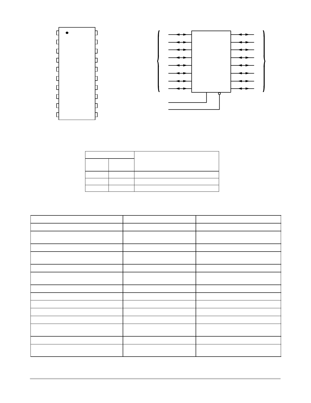
MC74HC245A
FUNCTION TABLE
Control Inputs
Output
Enable
Direction
L
L
L
H
H
X
X = don’t care
Operation
Data Transmitted from Bus B to Bus A
Data Transmitted from Bus A to Bus B
Buses Isolated (High−Impedance State)
MAXIMUM RATINGS (Note 1)
Symbol
Parameter
Value
Unit
VCC
VIN
VOUT
IIK
IOK
IOUT
ICC
IGND
TSTG
TL
TJ
qJA
DC Supply Voltage
DC Input Voltage
DC Output Voltage
DC Input Diode Current
DC Output Diode Current
DC Output Sink Current
DC Supply Current per Supply Pin
DC Ground Current per Ground Pin
Storage Temperature Range
Lead Temperature, 1 mm from Case for 10 Seconds
Junction Temperature Under Bias
Thermal Resistance
(Note 2)
SOIC
TSSOP
−0.5 to +7.0
−0.5 to VCC + 0.5
−0.5 to VCC + 0.5
±20
±35
±35
±75
±75
−65 to +150
260
+150
96
128
V
V
V
mA
mA
mA
mA
mA
_C
_C
_C
_C/W
PD
Power Dissipation in Still Air at 85_C
SOIC
500
mW
TSSOP
450
MSL Moisture Sensitivity
Level 1
FR
VESD
Flammability Rating
ESD Withstand Voltage
Oxygen Index: 30% to 35% UL 94 V−0 @ 0.125 in
Human Body Model (Note 3)
u2000
V
Machine Model (Note 4)
u200
Charged Device Model (Note 5)
u1000
ILATCHUP Latchup Performance
Above VCC and Below GND at 85_C (Note 6)
±300
mA
Stresses exceeding those listed in the Maximum Ratings table may damage the device. If any of these limits are exceeded, device functionality
should not be assumed, damage may occur and reliability may be affected.
1. Measured with minimum pad spacing on an FR4 board, using 10 mm−by−1 inch, 20 ounce copper trace with no air flow.
2. IO absolute maximum rating must observed.
3. Tested to EIA/JESD22−A114−A.
4. Tested to EIA/JESD22−A115−A.
5. Tested to JESD22−C101−A.
6. Tested to EIA/JESD78.
RECOMMENDED OPERATING CONDITIONS
Symbol
Parameter
Min
Max
Unit
VCC DC Supply Voltage (Referenced to GND)
2.0
6.0
V
Vin, Vout DC Input Voltage, Output Voltage (Referenced to GND)
0
VCC
V
TA
Operating Temperature, All Package Types
–55
+125
_C
tr, tf
Input Rise and Fall Time
(Figure 1)
VCC = 2.0 V
0
VCC = 4.5 V
0
VCC = 6.0 V
0
1000
ns
500
400
Functional operation above the stresses listed in the Recommended Operating Ranges is not implied. Extended exposure to stresses beyond
the Recommended Operating Ranges limits may affect device reliability.
http://onsemi.com
2
Share Link: 