MC14566B データシートの表示(PDF) - Motorola => Freescale
部品番号
コンポーネント説明
一致するリスト
MC14566B Datasheet PDF : 8 Pages
| |||
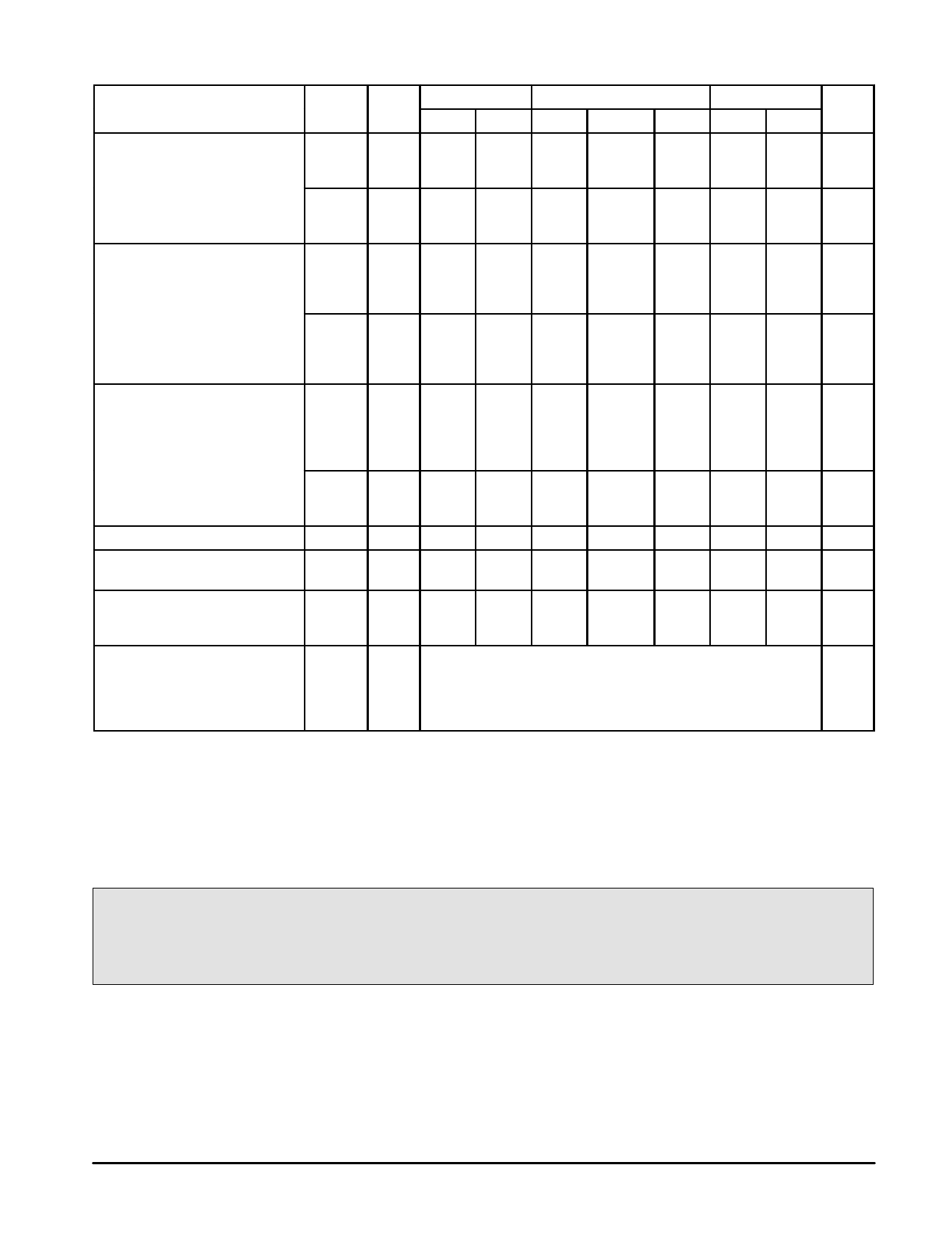
ÎÎÎÎEÎÎÎÎLEÎÎÎÎCTRÎÎÎÎICAÎÎÎÎL CÎÎÎÎHAÎÎÎÎRACÎÎÎÎTEÎÎÎÎRISÎÎÎÎTICÎÎÎÎS (VÎÎÎÎoltagÎÎÎÎesVRÎÎÎÎDefDeÎÎÎÎrencÎÎÎÎedtoÎÎÎΖV5S5ÎÎÎÎS_C) ÎÎÎÎÎÎÎÎÎÎÎÎÎÎÎÎÎÎÎÎ25_ÎÎÎÎC ÎÎÎÎÎÎÎÎÎÎÎÎÎÎÎÎÎÎÎÎ125ÎÎÎÎ_C ÎÎÎÎÎÎÎÎÎÎÎÎÎÎÎÎ
Characteristic
Symbol Vdc
Min
Max
Min
Typ #
Max
Min
Max Unit
Output Voltage
Vin = VDD or 0
“0” Level VOL
5.0
—
0.05
—
10
—
0.05
—
15
—
0.05
—
0
0.05
—
0.05 Vdc
0
0.05
—
0.05
0
0.05
—
0.05
Vin = 0 or VDD
“1” Level VOH
5.0
4.95
—
4.95
5.0
10
9.95
—
9.95
10
15
14.95
—
14.95
15
—
4.95
—
Vdc
—
9.95
—
—
14.95
—
Input Voltage
“0” Level VIL
(VO = 4.5 or 0.5 Vdc)
(VO = 9.0 or 1.0 Vdc)
(VO = 13.5 or 1.5 Vdc)
“1” Level VIH
(VO = 0.5 or 4.5 Vdc)
(VO = 1.0 or 9.0 Vdc)
(VO = 1.5 or 13.5 Vdc)
Output Drive Current
(VOH = 2.5 Vdc)
(VOH = 4.6 Vdc)
(VOH = 9.5 Vdc)
(VOH = 13.5 Vdc)
IOH
Source
5.0
—
1.5
—
2.25
10
—
3.0
—
4.50
15
—
4.0
—
6.75
5.0
3.5
—
3.5
2.75
10
7.0
—
7.0
5.50
15
11
—
11
8.25
5.0 – 3.0
—
– 2.4
– 4.2
5.0 – 0.64
—
– 0.51 – 0.88
10
– 1.6
—
– 1.3 – 2.25
15
– 4.2
—
– 3.4
– 8.8
Vdc
1.5
—
1.5
3.0
—
3.0
4.0
—
4.0
Vdc
—
3.5
—
—
7.0
—
—
11
—
mAdc
—
– 1.7
—
—
– 0.36
—
—
– 0.9
—
—
– 2.4
—
(VOL = 0.4 Vdc)
(VOL = 0.5 Vdc)
(VOL = 1.5 Vdc)
Input Current
Input Capacitance
(Vin = 0)
Quiescent Current
(Per Package)
Sink IOL
Iin
Cin
IDD
5.0
0.64
—
0.51
0.88
10
1.6
—
1.3
2.25
15
4.2
—
3.4
8.8
—
0.36
— mAdc
—
0.9
—
—
2.4
—
15
—
± 0.1
— ± 0.00001 ± 0.1
—
± 1.0 µAdc
—
—
—
—
5.0
7.5
—
—
pF
5.0
—
5.0
—
0.005
5.0
—
150 µAdc
10
—
10
—
0.010
10
—
300
15
—
20
—
0.015
20
—
600
Total Supply Current**†
(Dynamic plus Quiescent,
Per Package)
(CL = 50 pF on all outputs, all
buffers switching)
IT
5.0
10
15
IT = (1.0 µA/kHz) f + IDD
IT = (2.0 µA/kHz) f + IDD
IT = (3.0 µA/kHz) f + IDD
µAdc
#Data labelled “Typ” is not to be used for design purposes but is intended as an indication of the IC’s potential performance.
** The formulas given are for the typical characteristics only at 25_C.
†To calculate total supply current at loads other than 50 pF:
IT(CL) = IT(50 pF) + (CL – 50) Vfk
where: IT is in µA (per package), CL in pF, V = (VDD – VSS) in volts, f in kHz is input frequency, and k = 0.001.
This device contains protection circuitry to guard against damage due to high static voltages or electric fields. However,
precautions must be taken to avoid applications of any voltage higher than maximum rated voltages to this high-impedance
circuit. For proper operation, Vin and Vout should be constrained to the range VSS ≤ (Vin or Vout) ≤ VDD.
Unused inputs must always be tied to an appropriate logic voltage level (e.g., either VSS or VDD). Unused outputs must
be left open.
MC14566B
2
MOTOROLA CMOS LOGIC DATA
Share Link: 