MC100EP56(2004) データシートの表示(PDF) - ON Semiconductor
部品番号
コンポーネント説明
一致するリスト
MC100EP56 Datasheet PDF : 10 Pages
| |||
MC10EP56, MC100EP56
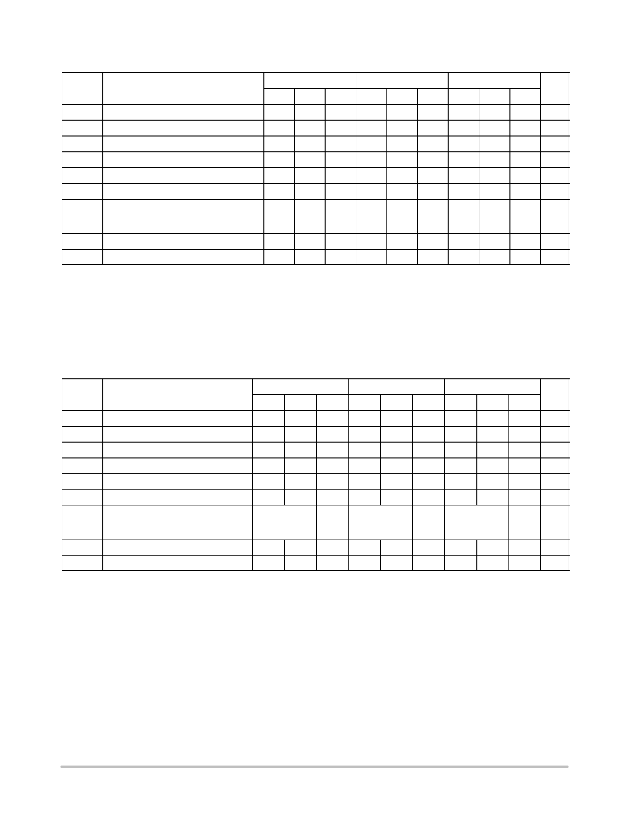
100EP DC CHARACTERISTICS, NECL VCC = 0 V, VEE = −5.5 V to −3.0 V (Note 18)
−40°C
25°C
85°C
Symbol
Characteristic
Min Typ Max Min Typ Max Min Typ Max Unit
IEE
VOH
VOL
VIH
VIL
VBB
VIHCMR
Power Supply Current
Output HIGH Voltage (Note 19)
Output LOW Voltage (Note 19)
Input HIGH Voltage (Single−Ended)
Input LOW Voltage (Single−Ended)
Output Voltage Reference
Input HIGH Voltage Common Mode
Range (Differential) (Note 20)
50
61
75
50
63
77
55
66
80 mA
−1145 −1020 −895 −1145 −1020 −895 −1145 −1020 −895 mV
−1945 −1820 −1695 −1945 −1820 −1695 −1945 −1820 −1695 mV
−1225
−880 −1225
−880 −1225
−880 mV
−1945
−1625 −1945
−1625 −1945
−1625 mV
−1525 −1425 −1325 −1525 −1425 −1325 −1525 −1425 −1325 mV
VEE+2.0
0.0
VEE+2.0
0.0
VEE+2.0
0.0
V
IIH
Input HIGH Current
150
150
150 mA
IIL
Input LOW Current
0.5
0.5
0.5
mA
NOTE: EP circuits are designed to meet the DC specifications shown in the above table after thermal equilibrium has been established. The
circuit is in a test socket or mounted on a printed circuit board and transverse airflow greater than 500lfpm is maintained.
18. Input and output parameters vary 1:1 with VCC.
19. All loading with 50 W to VCC−2.0 volts.
20. VIHCMR min varies 1:1 with VEE, VIHCMR max varies 1:1 with VCC. The VIHCMR range is referenced to the most positive side of the differential
input signal.
AC CHARACTERISTICS VCC = 0 V; VEE = −3.0 V to −5.5 V or VCC = 3.0 V to 5.5 V; VEE = 0 V (Note 21)
−40°C
25°C
85°C
Symbol
Characteristic
Min Typ Max Min Typ Max Min Typ Max Unit
fmax
tPLH,
tPHL
Maximum Frequency
(See Figure 2 Fmax/JITTER)
>3
>3
>3
GHz
Propagation Delay to
ps
Output Differential
D to Q, Q 250 340 450 270 360 470 300 400 500
SEL to Q, Q 250 340 450 270 340 470 300 400 500
COM_SEL to Q, Q 250 350 450 270 360 470 300 400 500
tSKEW
Within−Device Skew (Note 22)
Device to Device Skew
50 100
200
50 100
200
50 100 ps
200
tJITTER
Random Clock Jitter
(See Figure 2 Fmax/JITTER)
0.2 < 1
0.2 < 1
0.2 < 1 ps
VPP
Input Voltage Swing (Differential)
150 800 1200 150 800 1200 150 800 1200 mV
tr
Output Rise/Fall Times
tf
(20% − 80%)
Q, Q 70 120 170 80 130 180 100 150 230 ps
21. Measured using a 750 mV source, 50% duty cycle clock source. All loading with 50 W to VCC−2.0 V.
22. Skew is measured between outputs under identical transitions. Duty cycle skew is defined only for differential operation when the delays
are measured from the cross point of the inputs to the cross point of the outputs.
http://onsemi.com
6
Share Link: 