MB88151A データシートの表示(PDF) - Fujitsu
部品番号
コンポーネント説明
一致するリスト
MB88151A Datasheet PDF : 22 Pages
| |||
MB88151A
■ RECOMMENDED OPERATING CONDITIONS
Parameter
Power supply voltage
“H” level input voltage
“L” level input voltage
Input clock
duty cycle
Operating temperature
Symbol Pin Conditions
VDD
VDD
⎯
VIH
XIN,
⎯
SEL0,
VIL
SEL1,
⎯
ENS
tDCI
XIN
8.3 MHz to
33.4 MHz
Ta
⎯
⎯
Min
3.0
VDD × 0.8
VSS
40
− 40
Value
Typ
3.3
⎯
⎯
50
⎯
(VSS = 0.0 V)
Max
3.6
VDD + 0.3
Unit
V
V
VDD × 0.2
V
60
%
+ 85
°C
WARNING: The recommended operating conditions are required in order to ensure the normal operation of the
semiconductor device. All of the device’s electrical characteristics are warranted when the device is
operated within these ranges.
Always use semiconductor devices within their recommended operating condition ranges. Operation
outside these ranges may adversely affect reliability and could result in device failure.
No warranty is made with respect to uses, operating conditions, or combinations not represented on
the data sheet. Users considering application outside the listed conditions are advised to contact their
FUJITSU representatives beforehand.
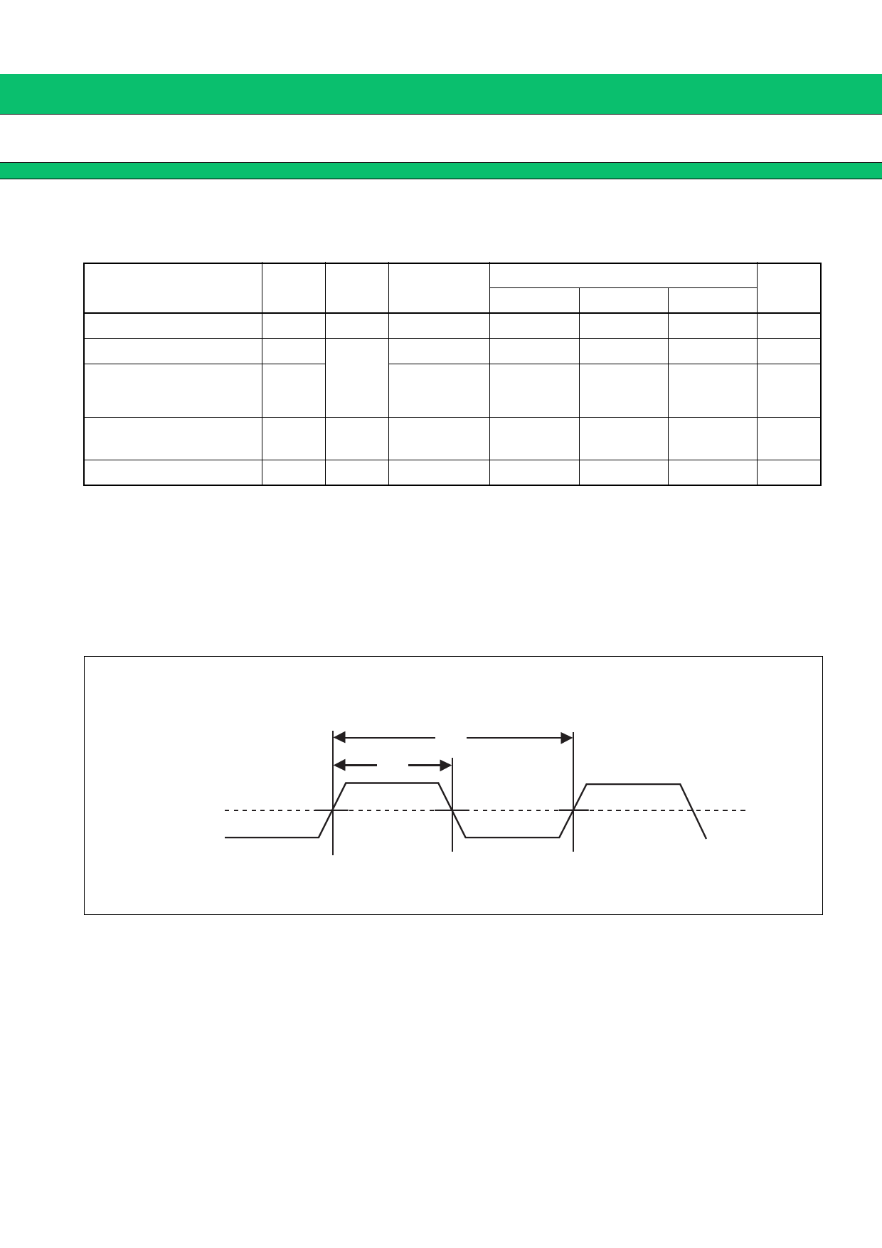
Input clock duty cycle (tDCI = tb/ta)
XIN
ta
tb
1.5 V
9
Share Link: 