MAX5915 データシートの表示(PDF) - Maxim Integrated
部品番号
コンポーネント説明
一致するリスト
MAX5915 Datasheet PDF : 25 Pages
| |||
Dual PCI 2.2 Hot-Swap Controllers
ABSOLUTE MAXIMUM RATINGS
+12VIN to GND ...................................................-0.3V to +14.0V
-12VIN to GND........................................................-14V to +0.3V
-12VO_ to GND......................................+0.3V to (V-12VIN - 0.3V)
+12VO_, 3.3VGATE_, 5VGATE_
to GND..................................................-0.3V to (V+12VIN + 0.3V)
Any Other Pin to GND ...........................................-0.3V to +6.0V
Continuous Power Dissipation (TA = +70°C)
28-Pin TSSOP (derate 23.8mW/°C above +70°C) ...........1.9W
Operating Temperature Ranges:
MAX591_U_ _ ......................................................0°C to +85°C
MAX591_A U_ _ ...................................................0°C to +85°C
MAX591_E_ _....................................................-40°C to +85°C
MAX591_ AE_ _ ................................................-40°C to +85°C
Maximum Junction Temperature .....................................+150°C
Storage Temperature Range .............................-65°C to +150°C
Lead Temperature (soldering, 10s) .................................+300°C
Stresses beyond those listed under “Absolute Maximum Ratings” may cause permanent damage to the device. These are stress ratings only, and functional
operation of the device at these or any other conditions beyond those indicated in the operational sections of the specifications is not implied. Exposure to
absolute maximum rating conditions for extended periods may affect device reliability.
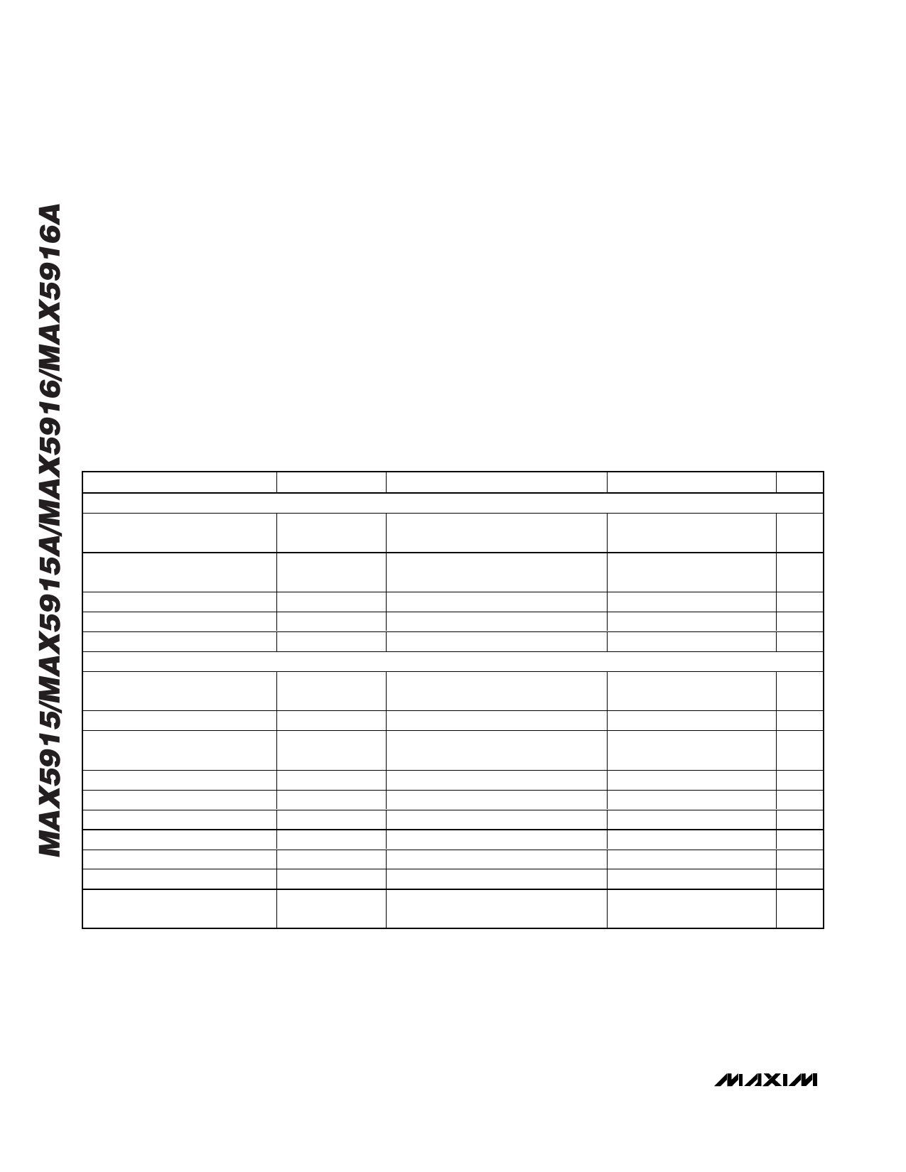
ELECTRICAL CHARACTERISTICS
(V-12VIN = -12V, V+12VIN = +12V, V3.3VAUXIN = +3.3V, VON_ = VAUXON_ = +5V, TA = TMIN to TMAX, unless otherwise specified.
Typical values are at TA = +25°C.)
PARAMETER
POWER SUPPLIES
SYMBOL
CONDITIONS
MIN
TYP MAX UNITS
Main Supply Input Voltage
Range
V+12VIN
10.8
12
13.2
V
Main Supply Undervoltage
Lockout (UVLO)
V+12UVLO
V+12VIN rising
9.6
10
10.8
V
Main Supply UVLO Hysteresis
Main Input UVLO Delay Time
Supply Current
+3.3V SUPPLY CONTROL
VUVLO, HYS
tDEG, UVLO
IQ
Figures 1 and 2 (Note 1)
100
mV
1.6
ms
2.5
5.0
mA
Gate Charge Current
Gate Discharge Current
Gate High Voltage
I3.3VGATE_, CHG
V3.3VGATE _ = +6V, V3.3VSEN_ = +3.3V,
V3.3VO_ = +3.3V
5
15
30
µA
I3.3VGATE_, DIS V3.3VGATE _ = +12V, VON_ = 0V
50
150
250
µA
V3.3VGATE_, HIGH I3.3VGATE _ = 1µA
V+12VIN -
0.5
V+12VIN
V
Gate Low Voltage
3.3VO_ Input Bias Current
3.3VO_ Internal Pulldown
3.3VSEN_ Input Bias Current
Current-Limit Threshold
Output Undervoltage Threshold
Output Undervoltage Threshold
Hysteresis
V3.3VGATE_, LOW
I3.3VO_, BIAS
RPD
I3.3VSEN_, BIAS
V3.3V, LIM
V3.3VIN, UV
I3.3VGATE _ = 1µA, VON_ = 0V
V3.3VO_ = +3.3V
VON_ = 0V
V3.3VSEN_ = +3.3V
V3.3VGATE _ = +6V
V3.3VGATE _ falling
0.1
0.4
V
20
µA
1
kΩ
10
µA
41
46
51
mV
2.79
2.89
2.99
V
30
mV
2 _______________________________________________________________________________________
Share Link: 