MAX4781 データシートの表示(PDF) - Maxim Integrated
部品番号
コンポーネント説明
一致するリスト
MAX4781 Datasheet PDF : 16 Pages
| |||
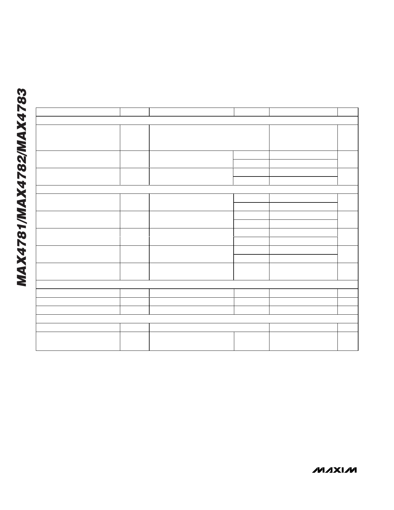
High-Speed, Low-Voltage, 0.7Ω CMOS Analog
Switches/Multiplexers
ELECTRICAL CHARACTERISTICS—Single +1.8V Supply
(VCC = +1.8V, GND = 0, VIH = 1V, VIL = 0.4V, TA = TMIN to TMAX, unless otherwise noted. Typical values are at TA = +25°C.) (Notes 2, 3)
PARAMETER
ANALOG SWITCH
SYMBOL
CONDITIONS
TA
MIN TYP MAX UNITS
Analog Signal Range
VX_, VY_,
VZ_, VX,
VY, VZ
0
VCC
V
On-Resistance (Note 4)
RON
On-Resistance Match Between
Channels (Notes 4, 5)
∆RON
SWITCH DYNAMIC CHARACTERISTICS
VCC = 1.8V; IX_, IY_, IZ_ = 10mA; +25°C
VX, VY, VZ = 1.0V
TMIN to TMAX
VCC = 1.8V; IX_, IY_, IZ_ = 10mA; +25°C
VX, VY, VZ = 1.0V
TMIN to TMAX
1.6
2.5
Ω
3.5
0.3
0.4
Ω
0.6
Turn-On Time
Turn-Off Time
Address Transition Time
Break-Before-Make Time
(Note 7)
tON
VX_, VY_, VZ_ = 1.0V; RL = 50Ω; +25°C
CL = 35pF; Figure 1
TMIN to TMAX
tOFF
VX_, VY_, VZ_ = 1.0V; RL = 50Ω; +25°C
CL = 35pF; Figure 1
TMIN to TMAX
tTRANS
VX_, VY_, VZ_ = 1.0V; RL = 50Ω; +25°C
CL = 35pF; Figure 2
TMIN to TMAX
tBBM
VX_, VY_, VZ_ = 1V; RL = 50Ω;
CL = 35pF; Figure 3
+25°C
TMIN to TMAX
1
17
30
ns
32
8
20
ns
22
17
30
ns
32
26
ns
Charge Injection
Q
VGEN = 0, RGEN = 0, CL = 1nF, +25°C
Figure 4
-40
pC
DIGITAL I/O
Input Logic High
Input Logic Low
Input Leakage Current
POWER SUPPLY
VIH
TMIN to TMAX
1
V
VIL
TMIN to TMAX
0.4
V
IIN_
VA, VB, VC = VENABLE = 0 or 3.6V TMIN to TMAX
-1 0.000
+1
µA
Power-Supply Range
VCC
1.6
3.6
V
Positive Supply Current
ICC
VCC = 3.6V; VA, VB, VC,
VENABLE = 0 or 3.6V
1
µA
Note 2: The algebraic convention is used in this data sheet; the most negative value is shown in the minimum column.
Note 3: Devices are tested at maximum hot temperature and are guaranteed by design and correlation at TA = +25°C and -40°C
specifications.
Note 4: RON and ∆RON matching specifications for thin QFN-packaged parts are guaranteed by design.
Note 5: ∆RON = RON(MAX) - RON(MIN).
Note 6: Flatness is defined as the difference between the maximum and minimum value of on-resistance as measured over the
specified analog signal ranges.
Note 7: Guaranteed by design; not production tested.
Note 8: Off-isolation = 20log10(VCOM_ / VNO), VCOM_ = output, VNO = input to off switch.
Note 9: Between any two channels.
4 _______________________________________________________________________________________
Share Link: 