MAX4135EWG(1996) データシートの表示(PDF) - Maxim Integrated
部品番号
コンポーネント説明
一致するリスト
MAX4135EWG Datasheet PDF : 12 Pages
| |||
1-Input/6-Output
Video Distribution Amplifiers
ABSOLUTE MAXIMUM RATINGS
Power-Supply Voltage (VCC to VEE).......................................12V
Voltage on Any Input Pin to GND .......(VCC + 0.3V) to (VEE - 0.3V)
Short-Circuit Duration to GND....................................Continuous
Continuous Power Dissipation (TA = +70°C)
Wide SO (derate 19.3mW/°C above +70°C)..................1.54W
Operating Temperature Range
MAX4135EWG/MAX4136EWG ........................-40°C to +85°C
Storage Temperature Range .............................-65°C to +160°C
Lead Temperature (soldering, 10sec) .............................+300°C
Stresses beyond those listed under “Absolute Maximum Ratings” may cause permanent damage to the device. These are stress ratings only, and functional
operation of the device at these or any other conditions beyond those indicated in the operational sections of the specifications is not implied. Exposure to
absolute maximum rating conditions for extended periods may affect device reliability.
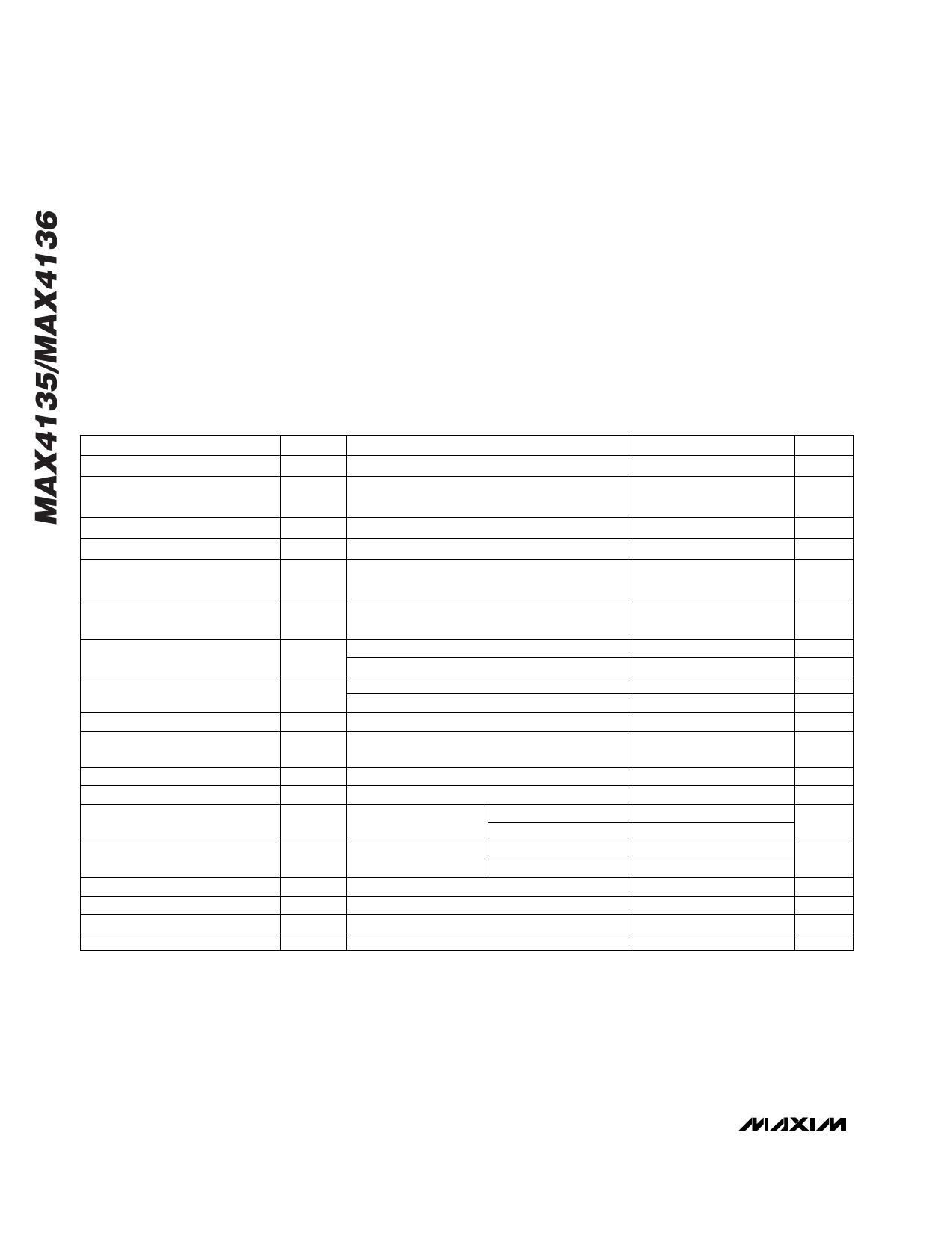
DC ELECTRICAL CHARACTERISTICS
(VCC = +5V, VEE = -5V, TA = TMIN to TMAX, unless otherwise noted. Typical values are at TA = +25°C.)
PARAMETER
SYMBOL
CONDITIONS
MIN
Input Offset Voltage
VOS VOUT = 0V, RL = ∞
Input Offset Voltage Match
Between Channels
VOUT = 0V, RL = ∞
Input Offset Voltage Drift
Input Bias Current
Common-Mode Input
Resistance
TCVOS
IB
VOUT = 0V, RL = 150Ω
VOUT = 0V, RL = 150Ω, VCM = 0V
RIN(CM) MAX4136, either input
Common-Mode Input
Capacitance
Input Voltage Noise
Input Current Noise
Input Capacitance
Common-Mode Input Voltage
Range
Common-Mode Rejection Ratio
Power-Supply Rejection Ratio
Quiescent Supply Current
Output Voltage Swing
Output Current Drive
SEL High Threshold
SEL Low Threshold
SEL Input Current
CIN(CM)
en
in
CIN
VCM
CMRR
PSRR
ISY
VOUT
IOUT
VIH
VIL
ISEL
MAX4136, either input
f = 1MHz
f = 1MHz to 100MHz
f = 1MHz
f = 1MHz to 100MHz
MAX4136
MAX4136, VCM = ±2.5V
VS = ±4.75V to ±5.25V
VIN = 0V
All channels off
All channels on
RL = 150Ω
Positive
Negative
RL = 30Ω
55
+2.2
-2.0
45
0.8
TYP
1
1
30
4.5
5
2
7
88
2.4
30
2
±2.5
60
65
45
70
+2.6
-2.5
65
1
MAX UNITS
8
mV
6
mV
µV/°C
10
µA
MΩ
pF
nV/√Hz
µVRMS
pA/√Hz
nARMS
pF
V
dB
dB
55
mA
80
V
mA
2.0
V
V
5
µA
2 _______________________________________________________________________________________
Share Link: 