MAX608ESA データシートの表示(PDF) - Maxim Integrated
部品番号
コンポーネント説明
一致するリスト
MAX608ESA Datasheet PDF : 12 Pages
| |||
5V or Adjustable, Low-Voltage,
Step-Up DC-DC Controller
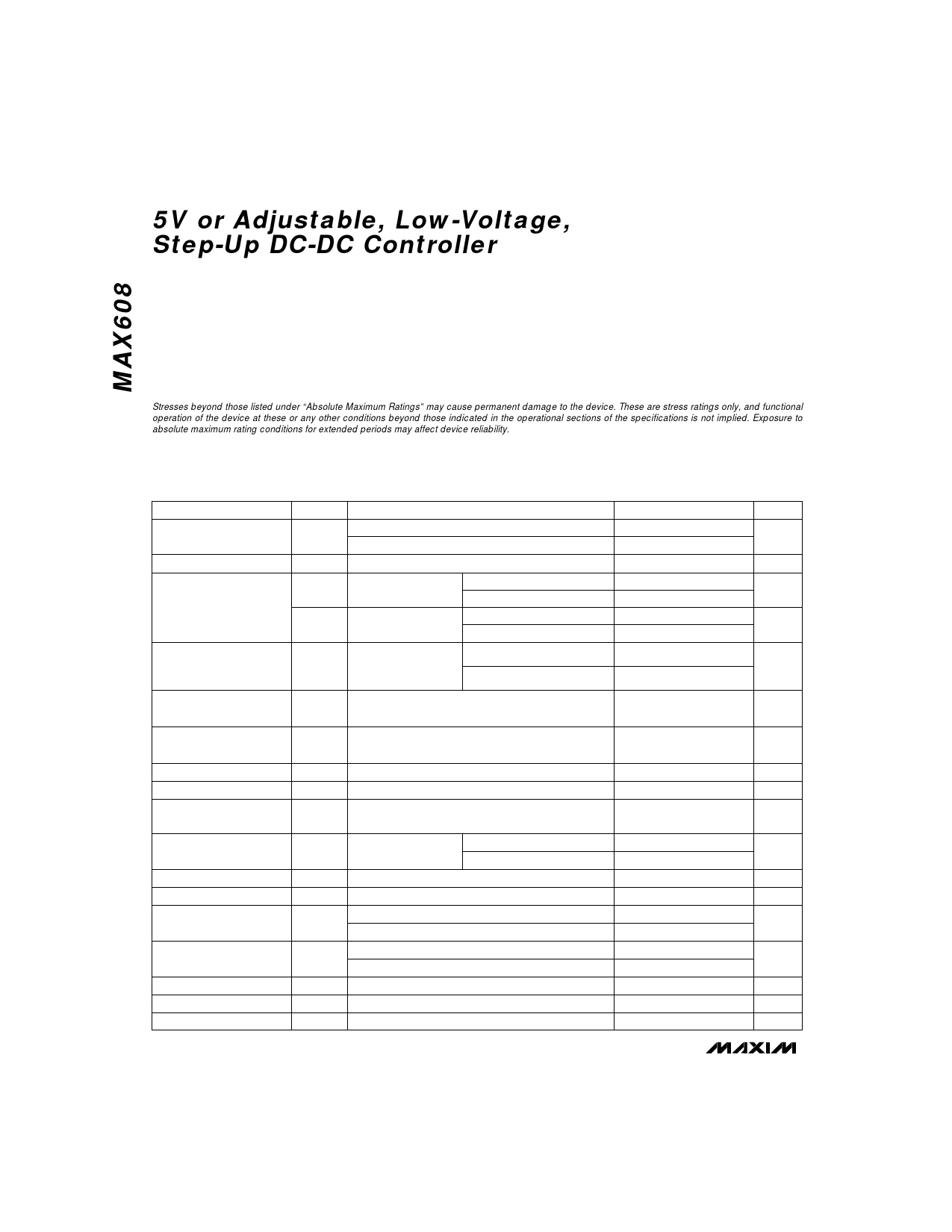
ABSOLUTE MAXIMUM RATINGS
Supply Voltage
OUT to GND.............................................................-0.3V, 17V
EXT, CS, REF, SHDN, FB to GND ...............-0.3V, (VOUT + 0.3V)
GND to AGND.............................................................0.1V, -0.1V
Continuous Power Dissipation (TA = +70°C)
Plastic DIP (derate 9.09mW/°C above +70°C) ............727mW
SO (derate 5.88mW/°C above +70°C) .........................471mW
Operating Temperature Range ...........................-40°C to +85°C
Junction Temperature ......................................................+150°C
Storage Temperature Range .............................-65°C to +160°C
Lead Temperature (soldering, 10sec) .............................+300°C
Stresses beyond those listed under “Absolute Maximum Ratings” may cause permanent damage to the device. These are stress ratings only, and functional
operation of the device at these or any other conditions beyond those indicated in the operational sections of the specifications is not implied. Exposure to
absolute maximum rating conditions for extended periods may affect device reliability.
ELECTRICAL CHARACTERISTICS
(VOUT = 5V, ILOAD = 0mA, TA = -40°C to +85°C where indicated. TA = -25°C to +85°C for all other limits. Typical values are at
TA = +25°C.)
PARAMETER
SYMBOL
CONDITIONS
MIN TYP MAX UNITS
Input Voltage Range
(Note 2)
TA = -25°C to +85°C
TA = -40°C to +85°C (Note 1)
1.8
16.5
V
1.9
16.5
Minimum Start-Up Voltage
No load
1.6
1.8
V
Supply Current
VOUT = 16.5V,
SHDN ≤ 0.4V
VOUT = 10V,
SHDN ≥ 1.6V
TA = -25°C to +85°C
TA = -40°C to +85°C (Note 1)
TA = -25°C to +85°C
TA = -40°C to +85°C (Note 1)
85
110
µA
120
2
5
µA
10
Output Voltage (Note 3)
VIN = 2.0V to 5.0V, TA = -25°C to +85°C
4.825 5.0 5.175
over full load range,
V
circuit of Figure 2a TA = -40°C to +85°C (Note 1) 4.800 5.0 5.200
Output Voltage Line
Regulation (Note 4)
VIN = 2.7V to 4.0V, VOUT = 5V, ILOAD = 500mA,
circuit of Figure 2a
7
mV/V
Output Voltage Load
Regulation (Note 4)
VIN = 2V, VOUT = 5V, ILOAD = 0mA to 500mA,
circuit of Figure 2a
Maximum Switch On-Time tON(max)
12
Minimum Switch Off-Time tOFF(min)
1.8
Efficiency
VIN = 4V, VOUT = 5V, ILOAD = 500mA,
circuit of Figure 2a
Reference Voltage
REF Load Regulation
REF Line Regulation
FB Trip Point Voltage
(Note 5)
FB Input Current
SHDN Input High Voltage
SHDN Input Low Voltage
SHDN Input Current
VREF
VFB
IFB
VIH
VIL
IIN
IREF = 0µA
TA = -25°C to +85°C
TA = -40°C to +85°C (Note 1)
0µA ≤ IREF ≤ 100µA
3V ≤ VOUT ≤ 16.5V
TA = -25°C to +85°C
TA = -40°C to +85°C (Note 1)
TA = -25°C to +85°C
TA = -40°C to +85°C (Note 1)
VOUT = 1.8V to 16.5V
VOUT = 1.8V to 16.5V
VOUT = 16.5V, SHDN = 0V or 16.5V
1.4625
1.4475
1.4625
1.4475
1.6
60
mV/A
16
20
µs
2.3
2.8
µs
87
%
1.5 1.5375
V
1.5525
-4
10
mV
40
100
µV/V
1.5 1.5375
V
1.5525
-4
±20
nA
±40
V
0.4
V
±1
µA
2 _______________________________________________________________________________________
Share Link: 