MIC39500-2.5BT(1999) データシートの表示(PDF) - Micrel
部品番号
コンポーネント説明
一致するリスト
MIC39500-2.5BT Datasheet PDF : 8 Pages
| |||
MIC39500/39501
Absolute Maximum Ratings (Note 1)
Supply Voltage (VIN) ..................................... –20V to +20V
Enable Voltage (VEN) .................................................. +20V
Storage Temperature (TS) ....................... –65°C to +150°C
Lead Temperature (soldering, 5 sec.) ....................... 260°C
ESD, Note 3
Micrel
Operating Ratings (Note 2)
Supply Voltage (VIN) .................................. +2.25V to +16V
Enable Voltage (VEN) .................................................. +16V
Maximum Power Dissipation (PD(max)) ..................... Note 4
Junction Temperature (TJ) ....................... –40°C to +125°C
Package Thermal Resistance
TO-263 (θJC) ......................................................... 2°C/W
TO-220 (θJC) ......................................................... 2°C/W
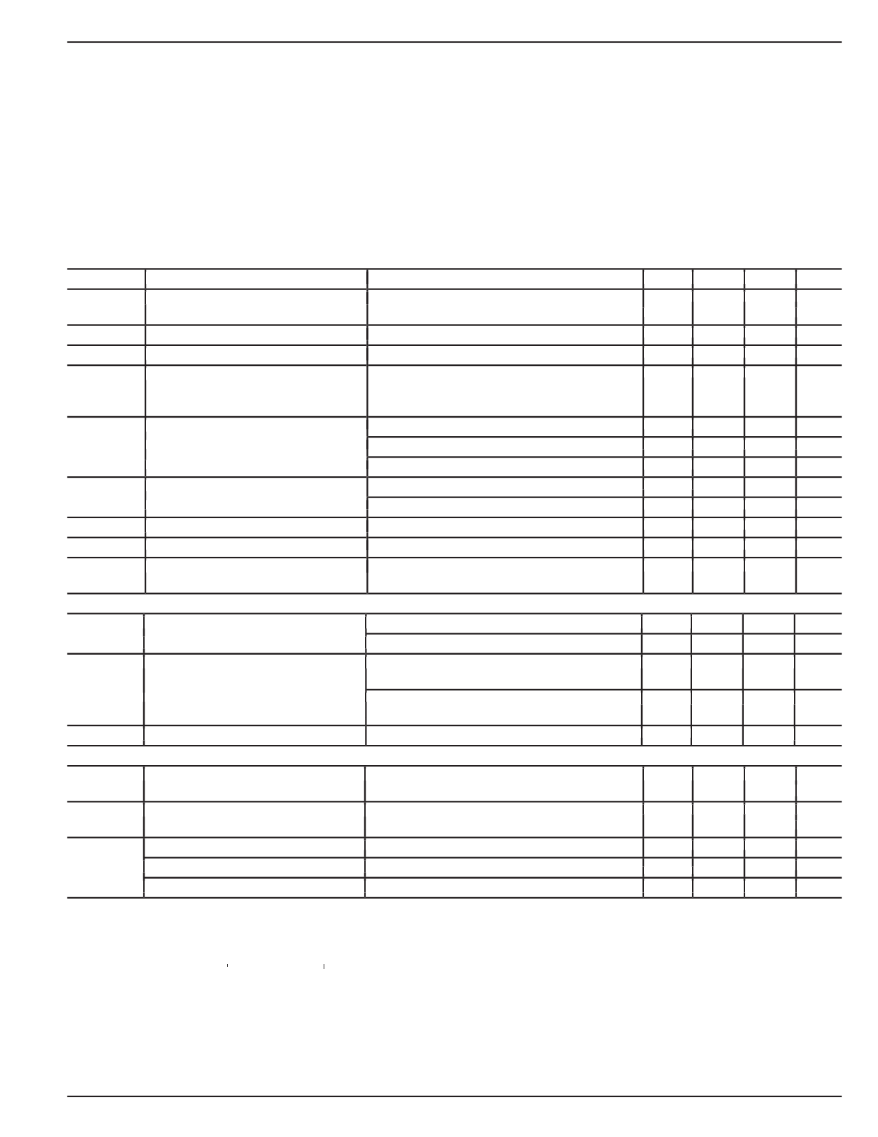
Electrical Characteristics
TJ = 25°C, bold values indicate –40°C ≤ TJ ≤ +125°C; unless noted
Symbol
Parameter
Condition
Min
VOUT
Output Voltage
10mA ≤ IOUT ≤ 5A, VOUT + 1V ≤ VIN ≤ 16V
–1
–2
∆VOUT/∆T
Line Regulation
Load Regulation
Output Voltage Temp. Coefficient,
Note 5
IOUT = 10mA, VOUT + 1V ≤ VIN ≤ 16V
VIN = VOUT + 1V, 10mA ≤ IOUT ≤ 5A
VDO
Dropout Voltage, Note 6
IGND
Ground Current, Note 7
IGND(do)
Dropout Ground Pin Current
IOUT(lim)
Current Limit
en
Output Noise Voltage
Enable Input (MIC39501)
IOUT = 250mA, ∆VOUT = –2%
IOUT = 2.5A, ∆VOUT = –2%
IOUT = 5A, ∆VOUT = –2%
IOUT = 2.5A, VIN = VOUT + 1V
IOUT = 5A, VIN = VOUT + 1V
VIN ≤ VOUT(nominal) – 0.5V, IOUT = 10mA
VOUT = 0V, VIN = VOUT + 1V
COUT = 47µF, IOUT = 100mA, 10Hz to 100kHz
VEN
Enable Input Voltage
logic low (off)
logic high (on)
2.4
IIN
Enable Input Current
VEN = VIN
VEN = 0.8V
IOUT(shdn)
Shutdown Output Current
Flag Output (MIC39501)
IFLG(leak)
Output Leakage Current
Note 8
VOH = 16V
VFLG(do)
Output Low Voltage
VIN = 2.250V, IOL, = 250µA, Note 9
Typ
0.06
0.2
20
125
320
400
15
70
2.1
7.5
260
30
10
0.01
125
Note 1.
Note 2.
Note 3.
Note 4.
Note 5.
Note 6.
Note 7.
Note 8.
Note 9.
Exceeding the absolute maximum ratings may damage the device.
The device is not guaranteed to function outside its operating rating.
Devices are ESD sensitive. Handling precautions recommended.
PD(max) = (TJ(max) – TA) ÷ θJA, where θJA depends upon the printed circuit layout. See “Applications Information.”
Output voltage temperature coefficient is ∆VOUT(worst case) ÷ (TJ(max) – TJ(min)) where TJ(max) is +125°C and TJ(min) is 0°C.
VDO = VIN – VOUT when VOUT decreases to 98% of its nominal output voltage with VIN = VOUT + 1V.
IGND is the quiescent current. IIN = IGND + IOUT.
VEN ≤ 0.8V, VIN ≤ 8V, and VOUT = 0V
For a 2.5V device, VIN = 2.250V (device is in dropout).
Max Units
1
%
2
%
0.5
%
1
%
100 ppm/°C
250 mV
mV
500 mV
50
mA
mA
mA
A
µV(rms)
0.8
V
V
35
µA
75
µA
2
µA
4
µA
20
µA
1
µA
2
µA
150 mV
200 mV
June 1999
3
MIC39500/39501
Share Link: 