M62216GP データシートの表示(PDF) - Renesas Electronics
部品番号
コンポーネント説明
一致するリスト
M62216GP Datasheet PDF : 12 Pages
| |||
M62216FP/GP
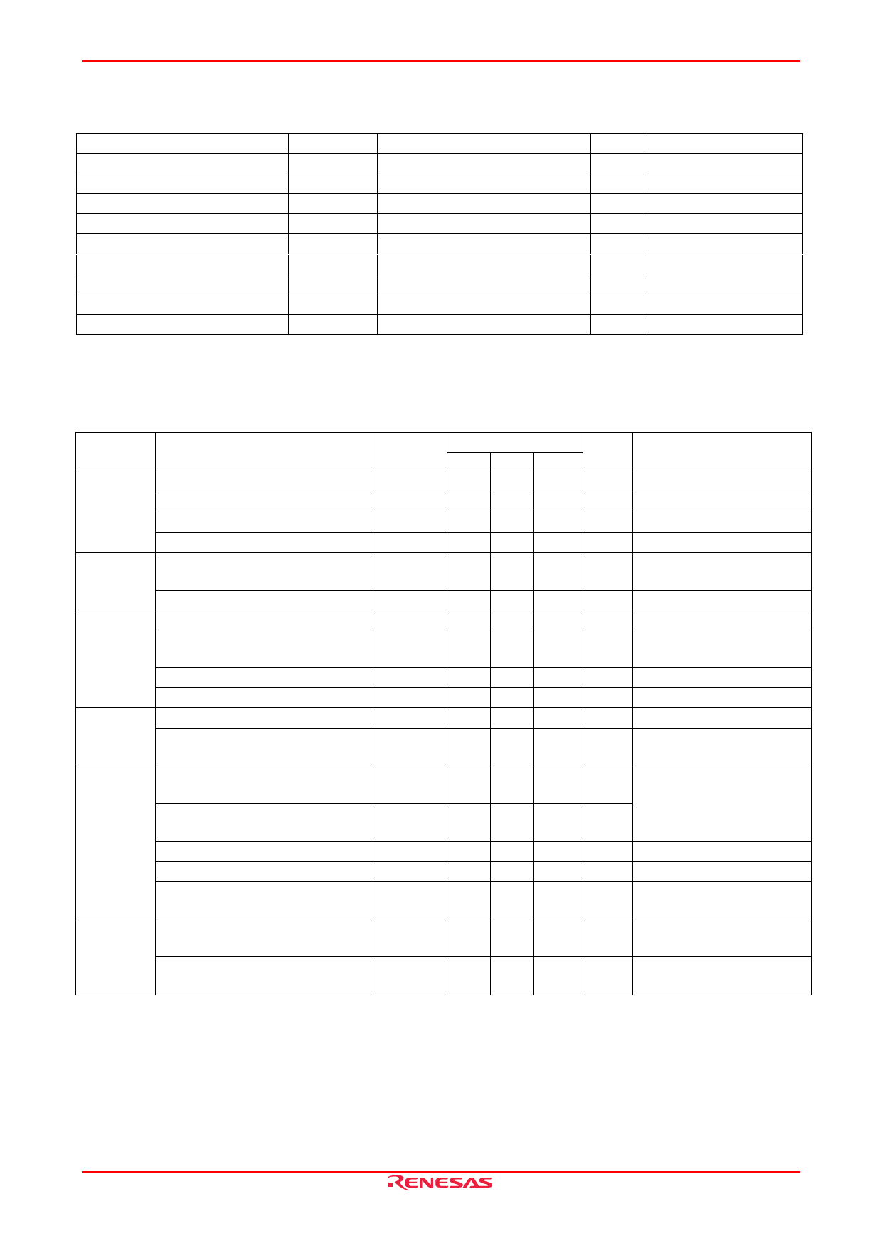
Absolute Maximum Ratings
Item
Input voltage
Bias terminal supply voltage
Drive1 terminal supply voltage
Drive2 terminal supply voltage
Drive1 terminal input current
Drive2 terminal Input current
Power dissipation
Operating temperature
Storage temperature
Symbol
VIN
VBlAS
VDRIVE1
VDRIVE2
IDRIVE1
IDRIVE2
Pd
Topr
Tstg
Ratings
15.5
15.5
15.5
15.5
100
10
440 (FP) 250 (GP)
−20 to +85
−40 to +150
(Ta = 25°C, unless otherwise noted)
Units
Conditions
V
V
V
V
mA
mA
mW Ta = 25°C
°C
°C
Electrical Characteristics
(Ta = 25°C, VIN = 1.7 V, VOUT = VBIAS = 3.0 V, unless otherwise noted)
Limits
Block
Item
Symbol Min Typ Max Units
Test Condition
All device
Voltage
reference
Input voltage range
BIAS voltage setting range*1
BIAS current
BIAS current at off mode
Reference voltage
VIN
VBlAS
IB
IB (OFF)
VREF
0.9 15
V
1.7 15
V
850 1200 µA
35 47 µA
1.20 1.26 1.32
V Use internal amp as
Buffer-amp
Error
Amp.
BIAS voltage regulation of VREF
Input current
Open loop voltage gain
∆VREF
IIN
AV
10 30 mV VBIAS = 1.7 to 15 V
20 nA IN = 1 V/IM
70
dB fIN = 100 Hz, null amp
operation
Osc.
FB terminal sink current
FB terminal source current
Oscillation frequency
Maximum on duty
IFB+
260 800 µA IN = 1.4 V, FB = 1.25 V/IM
IFB−
30 45 60 µA IN = 1.1 V, FB = 1.25 V/IM
fOSC
95 125 155 kHz PWM terminal monitored
DUTYmax 82 87
92
% PWM terminal monitored,
IN = 1.1 V
Output
Saturation voltage between PWM
Term. and DRIVE1 Term.
Saturation voltage between PWM
Term. and DRIVE2 Term.
Vsat1
Vsat2
0.25 0.5
1.0 1.2
V
IDRIVE1 = 50 mA,
IDRIVE2 = 5 mA
V
Leak current of DRIVE1 terminal
Leak current of DRIVE2 terminal
Output low voltage of PWM
terminal
IL1
IL2
VPWM (L)
−1
1
−1
1
0.03 0.3
µA IN = 1.4 V
µA IN = 1.4 V
V IPWM = 1 mA
ON/OFF
Input current of ON/OFF terminal ION
at on status
2
3
µA
Threshold voltage of ON/OFF
terminal
VTH (ON)
0.65 0.75 V
Note: 1. Setting range of BlAS voltage as same as setting range of output voltage.
REJ03D0845-0300 Rev.3.00 Jun 15, 2007
Page 3 of 11
Share Link: 