M37516E9-XXXHP データシートの表示(PDF) - Renesas Electronics
部品番号
コンポーネント説明
一致するリスト
M37516E9-XXXHP Datasheet PDF : 90 Pages
| |||
7516 Group
SERIAL I/O
qSERIAL I/O1
Serial I/O1 can be used as either clock synchronous or asynchro-
nous (UART) serial I/O. A dedicated timer is also provided for
baud rate generation.
(1) Clock Synchronous Serial I/O Mode
Clock synchronous serial I/O mode can be selected by setting the
serial I/O1 mode selection bit of the serial I/O1 control register (bit
6 of address 001A16) to “1”.
For clock synchronous serial I/O, the transmitter and the receiver
must use the same clock. If an internal clock is used, transfer is
started by a write signal to the TB/RB.
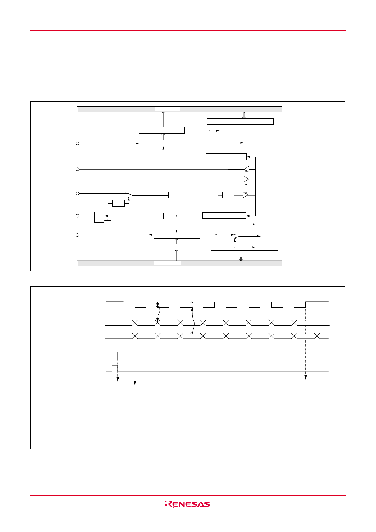
P24/RXD
Data bus
Address 001816
Receive buffer register
Serial I/O1 control register Address 001A16
Receive buffer full flag (RBF)
Receive shift register
Shift clock
Receive interrupt request (RI)
Clock control circuit
P26/SCLK
BRG count source selection bit
XIN
1/4
Serial I/O1 synchronous
clock selection bit
Frequency division ratio 1/(n+1)
Baud rate generator 1/4
Address 001C16
P27/SRDY1
P25/TXD
F/F
Falling-edge detector
Clock control circuit
Shift clock
Transmit shift completion flag (TSC)
Transmit shift register
Transmit interrupt source selection bit
Transmit interrupt request (TI)
Transmit buffer register
Address 001816
Data bus
Transmit buffer empty flag (TBE)
Serial I/O1 status register Address 001916
Fig. 18 Block diagram of clock synchronous serial I/O1
Transfer shift clock
(1/2 to 1/2048 of the internal
clock, or an external clock)
Serial output TxD
Serial input RxD
D0
D1
D2
D0
D1
D2
D3
D4
D5
D6
D7
D3
D4
D5
D6
D7
Receive enable signal SRDY1
Write pulse to receive/transmit
buffer register (address 001816)
TBE = 0
TBE = 1
TSC = 0
RBF = 1
TSC = 1
Overrun error (OE)
detection
Notes 1: As the transmit interrupt (TI), either when the transmit buffer has emptied (TBE=1) or after the transmit shift operation has
ended (TSC=1), by setting the transmit interrupt source selection bit (TIC) of the serial I/O1 control register.
2: If data is written to the transmit buffer register when TSC=0, the transmit clock is generated continuously and serial data
is output continuously from the TxD pin.
3: The receive interrupt (RI) is set when the receive buffer full flag (RBF) becomes “1” .
Fig. 19 Operation of clock synchronous serial I/O1 function
Rev.1.01 Jul 01, 2003 page 22 of 89
Share Link: 