SSR1N50B データシートの表示(PDF) - Fairchild Semiconductor
部品番号
コンポーネント説明
一致するリスト
SSR1N50B Datasheet PDF : 9 Pages
| |||
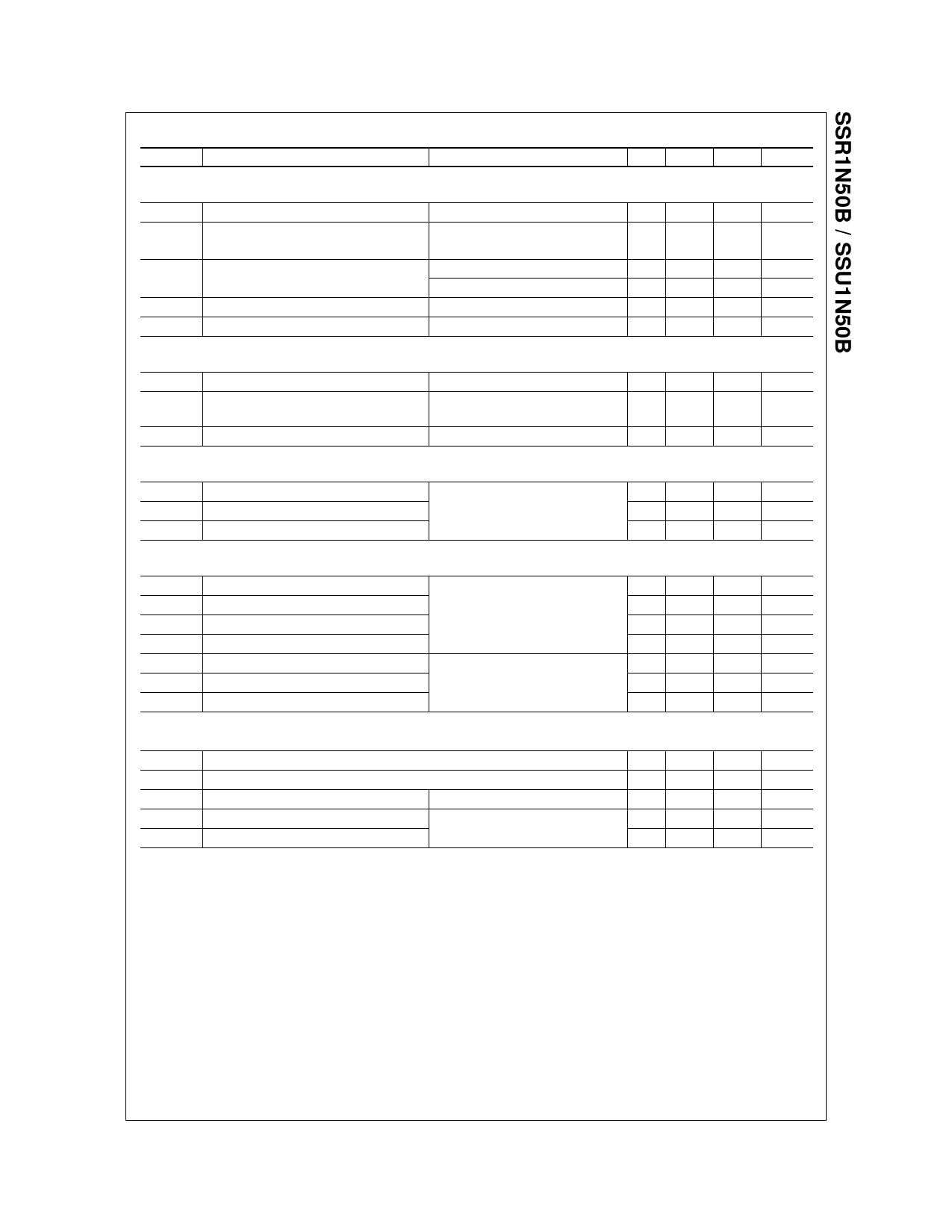
Electrical Characteristics
Symbol
Parameter
TC = 25°C unless otherwise noted
Test Conditions
Min Typ Max Units
Off Characteristics
BVDSS
∆BVDSS
/ ∆TJ
Drain-Source Breakdown Voltage
Breakdown Voltage Temperature
Coefficient
VGS = 0 V, ID = 250 µA
520 --
ID = 250 µA, Referenced to 25°C -- 0.54
IDSS
Zero Gate Voltage Drain Current
VDS = 520 V, VGS = 0 V
VDS = 400 V, TC = 125°C
--
--
--
--
IGSSF
IGSSR
Gate-Body Leakage Current, Forward VGS = 30 V, VDS = 0 V
Gate-Body Leakage Current, Reverse VGS = -30 V, VDS = 0 V
--
--
--
--
On Characteristics
VGS(th)
RDS(on)
Gate Threshold Voltage
Static Drain-Source
On-Resistance
gFS
Forward Transconductance
VDS = VGS, ID = 250 µA
VGS = 10 V, ID = 0.65 A
VDS = 40 V, ID = 0.65 A
2.0 --
-- 4.1
-- 1.65
Dynamic Characteristics
Ciss
Input Capacitance
Coss
Output Capacitance
Crss
Reverse Transfer Capacitance
VDS = 25 V, VGS = 0 V,
f = 1.0 MHz
-- 260
-- 25
-- 5.5
Switching Characteristics
td(on)
Turn-On Delay Time
tr
Turn-On Rise Time
td(off)
Turn-Off Delay Time
tf
Turn-Off Fall Time
Qg
Total Gate Charge
Qgs
Gate-Source Charge
Qgd
Gate-Drain Charge
VDD = 250 V, ID = 1.5 A,
RG = 25 Ω
VDS = 400 V, ID = 1.5 A,
VGS = 10 V
-- 14
-- 40
-- 35
-- 35
-- 8.3
-- 1.5
-- 3.4
--
--
10
100
100
-100
4.0
5.3
--
340
33
7.2
40
90
80
80
11
--
--
V
V/°C
µA
µA
nA
nA
V
Ω
S
pF
pF
pF
ns
ns
ns
ns
nC
nC
nC
Drain-Source Diode Characteristics and Maximum Ratings
IS
Maximum Continuous Drain-Source Diode Forward Current
ISM
Maximum Pulsed Drain-Source Diode Forward Current
VSD
Drain-Source Diode Forward Voltage VGS = 0 V, IS = 1.3 A
trr
Reverse Recovery Time
Qrr
Reverse Recovery Charge
VGS = 0 V, IS = 1.5 A,
dIF / dt = 100 A/µs
Notes:
1. Repetitive Rating : Pulse width limited by maximum junction temperature
2. L = 106mH, IAS = 1.5A, VDD = 50V, RG = 25 Ω, Starting TJ = 25°C
3. ISD ≤ 1.5A, di/dt ≤ 300A/µs, VDD ≤ BVDSS, Starting TJ = 25°C
4. Pulse Test : Pulse width ≤ 300µs, Duty cycle ≤ 2%
5. Essentially independent of operating temperature
--
--
1.3
A
--
--
5.0
A
--
--
1.4
V
-- 230
--
ns
-- 0.94 --
µC
©2002 Fairchild Semiconductor Corporation
Rev. C, May 2002
Share Link: 