SC1565I5T-1.8_00 データシートの表示(PDF) - Semtech Corporation
部品番号
コンポーネント説明
一致するリスト
SC1565I5T-1.8_00 Datasheet PDF : 10 Pages
| |||
VERY LOW DROPOUT 1.5 AMP
REGULATOR WITH ENABLE
SC1565
October 3, 2000
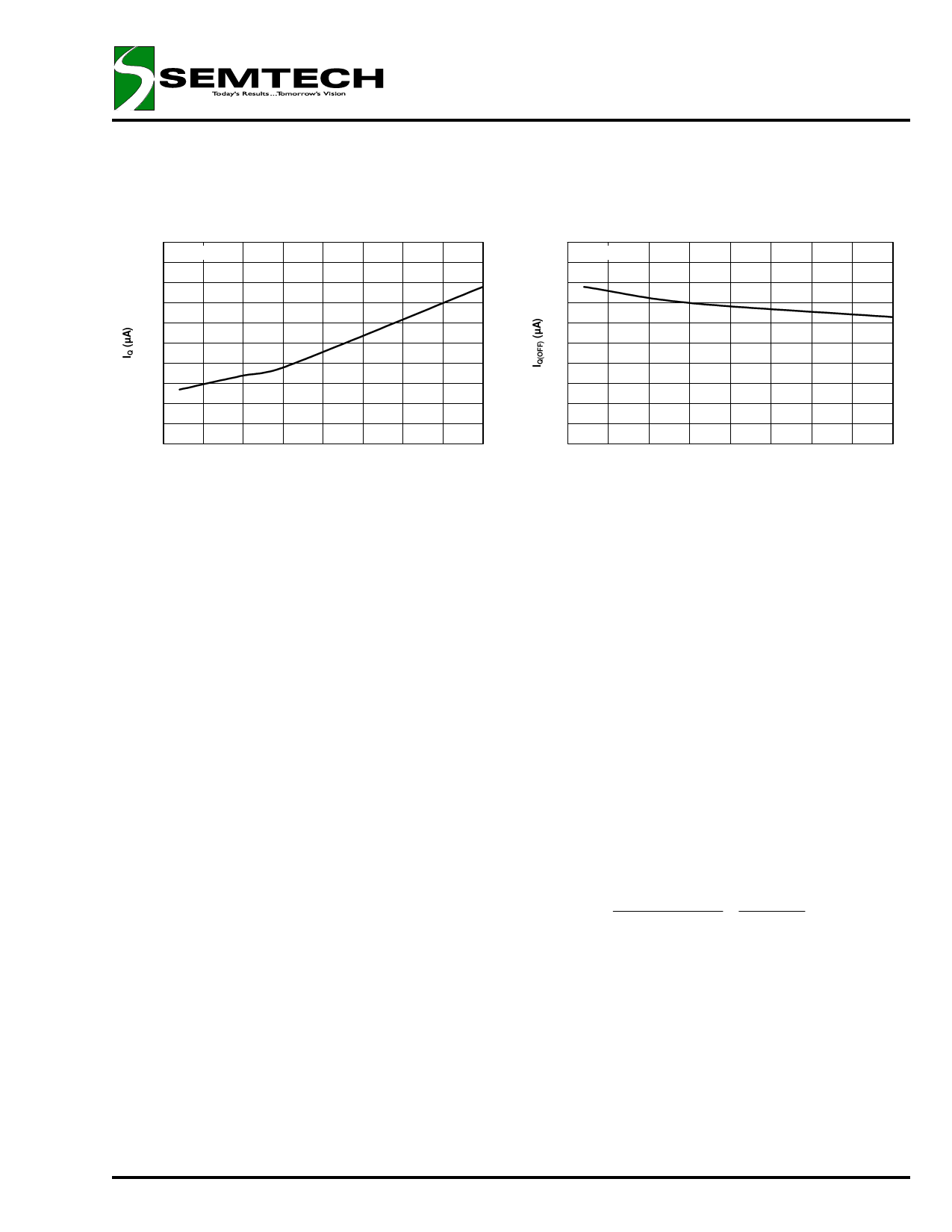
TYPICAL CHARACTERISTICS (Cont.)
Quiescent Current vs.
Junction Temperature
600
VIN = 3.3V
590
580
570
560
550
540
530
520
510
500
-50 -25
0
25
50
75
TJ (°C)
100 125 150
APPLICATIONS INFORMATION
Introduction
The SC1565 is intended for applications such as
graphics cards where high current capability and very
low dropout voltage are required. It provides a very
simple, low cost solution that uses very little pcb real
estate. Additional features include an enable pin to al-
low for a very low power consumption standby mode,
and a fully adjustable output.
Component Selection
Input capacitor - a 4.7µF ceramic capacitor is recom-
mended. This allows for the device being some dis-
tance from any bulk capacitance on the rail. Addition-
ally, input droop due to load transients is reduced, im-
proving load transient response. Additional capaci-
tance may be added if required by the application.
Output capacitor - a minimum bulk capacitance of
10µF, along with a 0.1µF ceramic decoupling capacitor
is recommended. Increasing the bulk capacitance will
improve the overall transient response. The use of
multiple lower value ceramic capacitors in parallel to
achieve the desired bulk capacitance will not cause
stability issues. Although designed for use with ce-
ramic output capacitors, the SC1565 is extremely toler-
ant of output capacitor ESR values and thus will also
work comfortably with tantalum output capacitors.
External voltage selection resistors - the use of 1% re-
sistors, and designing for a current flow ≥ 10µA is rec-
ommended to ensure a well regulated output (thus R2
≤ 120kΩ).
Off-State Quiescent Current vs.
Junction Temperature
10
VIN = 5.5V
9
8
7
6
5
4
3
2
1
0
-50 -25
0
25
50
75
100 125 150
TJ (°C)
Thermal Considerations
The power dissipation in the SC1565 is approximately
equal to the product of the output current and the input
to output voltage differential:
PD ≈ (VIN − VOUT ) • IO
The absolute worst-case dissipation is given by:
( ) PD (MAX ) = VIN (MAX ) − VOUT (MIN ) • IO (MAX ) + VIN (MAX ) • IQ(MAX )
For a typical scenario, VIN = 3.3V ± 5%, VOUT = 2.8V
and IO = 1.5A, therefore:
VIN(MAX) = 3.465V, VOUT(MIN) = 2.744V and
IQ(MAX) = 1.75mA,
Thus PD(MAX) = 1.09W.
Using this figure, and assuming TA(MAX) = 70°C, we can
calculate the maximum thermal impedance allowable
to maintain TJ ≤ 150°C:
( ) TJ(MAX ) − TA(MAX) (150 − 70)
R = TH(J− A )(MAX )
PD(MAX )
= 1.09 = 73.4° C / W
This should be achievable for the SO-8 package using
pcb copper area to aid in conducting the heat away,
such as one square inch of copper connected to the
ground pins of the device. The SOT-223 and TO-220
packages would not require heatsinking. Internal
ground/power planes and air flow will also assist in re-
moving heat. For higher ambient temperatures it may
be necessary to use additional copper area.
© 2000 SEMTECH CORP.
7
652 MITCHELL ROAD NEWBURY PARK CA 91320
Share Link: 