LT5537 データシートの表示(PDF) - Linear Technology
部品番号
コンポーネント説明
一致するリスト
LT5537 Datasheet PDF : 16 Pages
| |||
LT5537
PI FU CTIO S
ENBL (Pin 1): Enable Pin. When the input voltage is higher
than 1V, the circuit is ON. When the input voltage is less than
0.3V, or this pin is not connected, the chip is disabled (OFF).
IN+, IN– (Pins 2, 3): Differential Signal Input Pins. These
pins are internally biased to VCC – 0.4V. The impedance
between IN+ and IN– is approximately 1.73kΩ//1.45pF at
200MHz. The input pins should be AC coupled.
CAP+, CAP– (Pins 4, 5): External Filter Capacitor Pins. The
minimum RF input frequency can be lowered by adding an
optional external capacitor between CAP+ and CAP–.
VCC (Pin 6): Power Supply Pin. This pin should be decoupled
using 1000pF and 0.1µF capacitors.
VEE (Pin 7): Ground pin.
OUT (Pin 8): Output pin.
Exposed Pad (Pin 9): Should be connected to PCB ground.
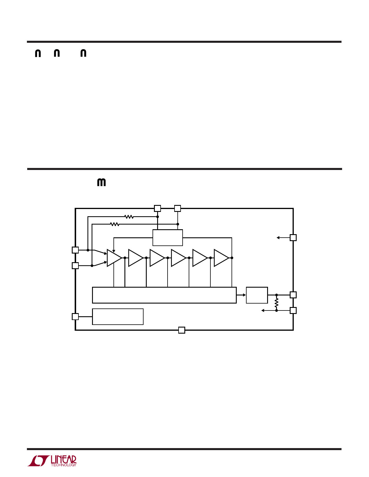
BLOCK DIAGRA
IN+
2
IN–
3
7k
7k
4
CAP+
5
CAP–
OFFSET
CANCELLATION
DETECTOR CELLS
ENBL
1
BANDGAP REFERENCE
AND BIASING
EXPOSED PAD
7
VCC
6
OUTPUT
BUFFER
OUT
8
7.2k
VEE
7
5537 BD
5537fa
7
Share Link: 