LT5503(RevA) データシートの表示(PDF) - Linear Technology
部品番号
コンポーネント説明
一致するリスト
LT5503 Datasheet PDF : 22 Pages
| |||
LT5503
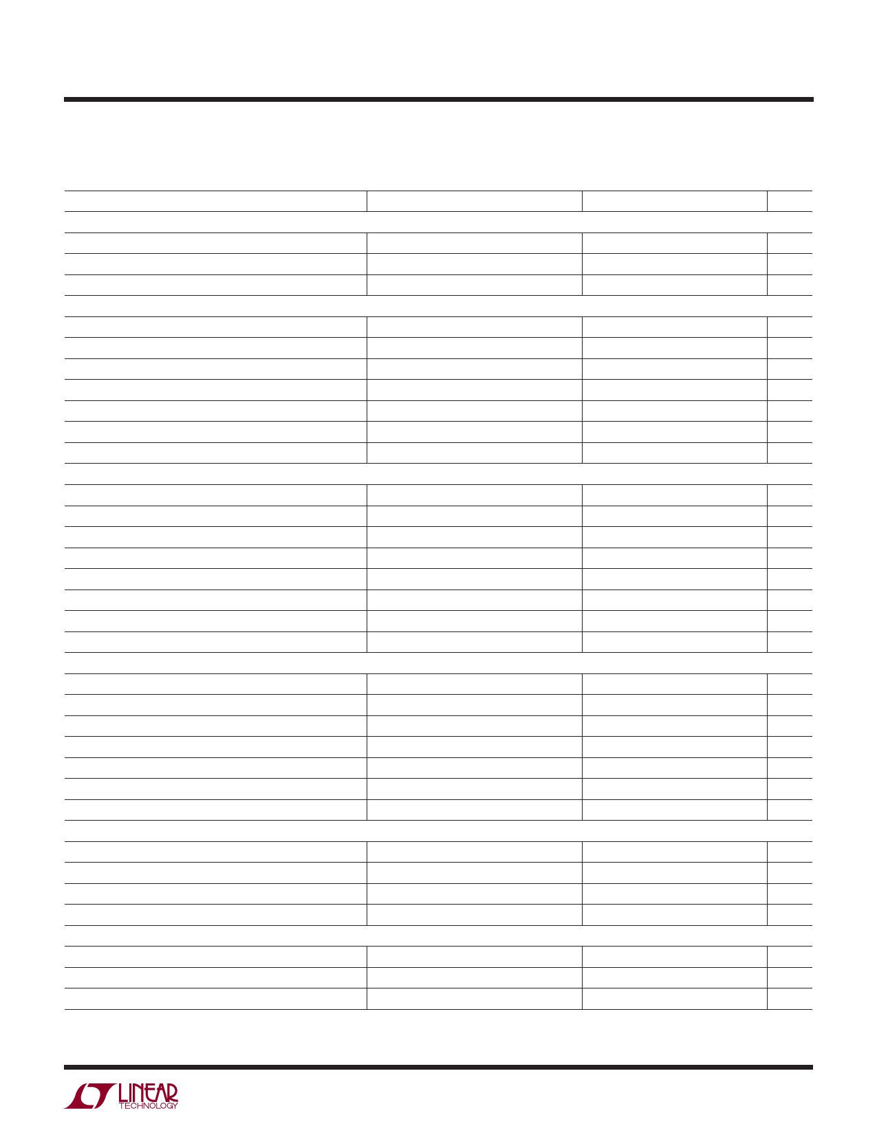
Electrical Characteristics (I/Q Modulator)
VCC1 = 3VDC, 2.4GHz matching, MODEN = High, GC1 = GC2 = Low, TA = 25°C, MODRFIN = 2.45GHz at –16dBm, [I – IB] and [Q – QB] =
100kHz CW signal at 1VP-P differential, Q leads I by 90°, unless otherwise noted. (Test circuit shown in Figure 2.) (Note 3)
PARAMETER
RF Carrier Input (MODRFIN)
Frequency Range2
Input VSWR
Input Power
Baseband Inputs (BI+, BI–, BQ+, BQ–)
Frequency Bandwidth (3dB)
Differential Input Voltage for 1dB Compressed Output
DC Common Mode Voltage
Differential Input Resistance
Input Capacitance
Gain Error
Phase Error
Modulated RF Carrier Output (MODRFOUT)
Output Power, Max Gain
Output VSWR
Image Suppression
Carrier Suppression
Output 1dB Compression
Output 3rd Order Intercept
Output 2rd Order Intercept
Broadband Noise
VGA Control Logic (GC2, GC1)
Switching Time
Input Current
Input Low Voltage
Input High Voltage
Output Power Attenuation
Output Power Attenuation
Output Power Attenuation
Modulator Enable (MODEN) Low = Off, High = On
Turn ON/OFF Time
Input Current
Enable
Disable
Modulator Power Supply Requirements
Supply Voltage
Modulator Supply Current
Modulator Shutdown Current
CONDITIONS
Requires Appropriate Matching
ZO = 50Ω
Internally Biased
ZO = 50Ω
f1 = 100kHz, fQ = 120kHz
f1 = 100kHz, fQ = 120kHz
20MHz Offset
GC2 = Low, GC1 = High
GC2 = High, GC1 = Low
GC2 = High, GC1 = High
MODEN = High
MODEN = Low
MIN
TYP
MAX
UNITS
1.2 to 2.7
GHz
1.3:1
–20 to –10
dBm
120
MHz
1
VP-P
1.4
VDC
18
kΩ
0.8
pF
±0.2
dB
±1
DEG
–6
–3
1.5:1
–26
–34
–24
–32
–3
2
16
–142
dBm
dBc
dBc
dBm
dBm
dBm
dBm/Hz
100
ns
2
µA
0.4
VDC
1.7
VDC
4.5
dB
9
dB
13.5
dB
1
µs
105
µA
VCC – 0.4
VDC
0.4
VDC
1.8
5.25
VDC
29
38
mA
50
µA
For more information www.linear.com/LT5503
5503fa
3
Share Link: 