LT3782AIFE(RevC) データシートの表示(PDF) - Linear Technology
部品番号
コンポーネント説明
一致するリスト
LT3782AIFE Datasheet PDF : 20 Pages
| |||
LT3782A
APPLICATIONS INFORMATION
Slope Compensation
The LT3782A is designed for high voltage and/or high
current applications, and very often these applications
generate noise spikes that can be picked up by the cur-
rent sensing amplifier and cause switching jitter. To avoid
switching jitter, careful layout is absolutely necessary to
minimize the current sensing noise pickup. Sometimes
increasing slope compensation to overcome the noise
can help to reduce jitter. The built-in slope compensa-
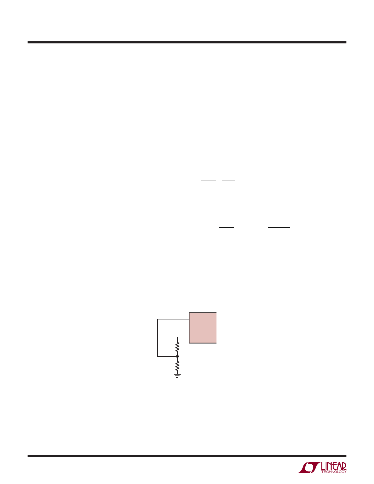
tion can be increased by adding a resistor RSLOPE from
SLOPE pin to ground. Note that smaller RSLOPE increases
slope compensation and the minimum RSLOPE allowed is
RFREQ/2.
Layout Considerations
To prevent EMI, the power MOSFETs and input bypass
capacitor leads should be kept as short as possible. A
ground plane should be used under the switching circuitry
to prevent interplane coupling and to act as a thermal
spreading path. Note that the bottom pad of the package
is the heat sink, as well as the IC signal ground, and must
be soldered to the ground plane.
In a boost converter, the conversion gain (assuming 100%
efficiency) is calculated as (ignoring the forward voltage
drop of the boost diode):
VOUT = 1
VIN 1−D
where D is the duty ratio of the main switch. D can then
be estimated from the input and output voltages:
D = 1−
VIN
VOUT
; DMAX
=
1−
VIN(MIN)
VOUT
The Peak and Average Input Currents
The control circuit in the LT3782A measures the input
current by using a sense resistor in each MOSFET source,
so the output current needs to be reflected back to the
input in order to dimension the power MOSFET properly.
Based on the fact that, ideally, the output power is equal
to the input power, the maximum average input current is:
IIN(MAX )
=
IO(MAX )
1– DMAX
The peak current is:
IIN(PEAK )
=
1.2
•
IO(MAX )
1– DMAX
The maximum duty cycle, DMAX, should be calculated at
minimum VIN.
Power Inductor Selection
In a boost circuit, a power inductor should be designed
to carry the maximum input DC current. The inductance
should be small enough to generate enough ripple current
to provide adequate signal to noise ratio to the LT3782A.
An empirical starting of the inductor ripple current (per
phase) is about 40% of maximum DC current, which is
half of the input DC current in a 2-phase circuit:
ΔIL
≅ 40% • IOUT(MAX) • VOUT
2VIN
= 20% • IOUT(MAX) •
VIN
VOUT
where VIN, VOUT and IOUT are the DC input voltage, output
voltage and output current, respectively.
And the inductance is estimated to be:
L = VIN • D
fs • ΔIL
where fs is the switching frequency per phase.
The saturation current level of inductor is estimated to be:
ISAT
≥
ΔIL
2
+ IIN
2
≅ 70% • IOUT(MAX) • VOUT
VIN(MIN)
10
For more information www.linear.com/LT3782A
3782afc
Share Link: 