3509 データシートの表示(PDF) - Linear Technology
部品番号
コンポーネント説明
一致するリスト
3509 Datasheet PDF : 24 Pages
| |||
LT3509
APPLICATIONS INFORMATION
In any step-down switcher the duty cycle when operating
in continuous, or fixed frequency, mode is dependent
on the step-down ratio. This is because for a constant
average load current the decay of the inductor current
when the switch is off must match the increase in inductor
current when the switch is on. The can be estimated by
the following formula:
DC
=
VOUT + VF
VIN − VSW + VF
where:
DC = Duty Cycle (Fraction of Cycle when Switch is On)
VOUT = Output Voltage
VIN = Input Voltage
VF = Catch Diode Forward Voltage
VSW = Switch Voltage Drop
Note: This formula neglects switching and inductor losses
so in practice the duty cycle may be slightly higher.
It is clear from this equation that the duty cycle will approach
100% as the input voltage is reduced and become smaller
as the input voltage increases. There are practical limits to
the minimum and maximum duty cycles for continuous
operation due to the switch minimum off and on times.
These are independent of operating frequency so it is clear
that range of usable duty cycle is inverserly proportional to
frequency. Therefore at higher frequency the input voltage
range (for constant frequency operation) will narrow.
The minimum duty cycle is given by:
DCMIN = fSW • tON(MIN)
where:
fSW = Switching Frequency
tON(MIN) = Switch Minimum On-Time
The minimum on time increases with increasing tempera-
ture so the value for the maximum operating temperature
should be used. See the Minimum On-Time vs Temperature
graph in the Typical Performance Characteristics.
The maximum input voltage for this duty cycle is given by:
VIN(MAX)
=
VOUT + VF
DCMIN
−
VF
+
VSW
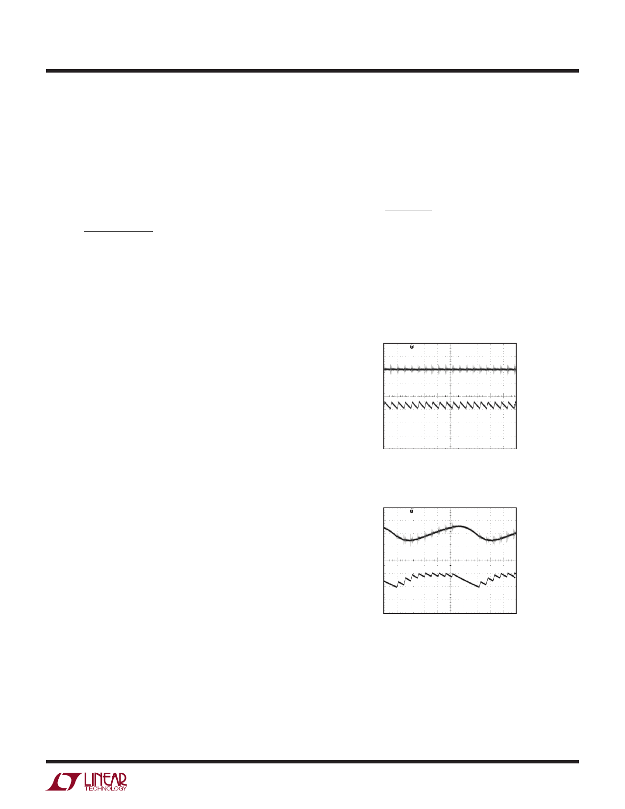
Above this voltage the only way the LT3509 can maintain
regulation is to skip cycles so the effective frequency will
reduce. This will cause an increase in ripple and the switch-
ing noise will shift to a lower frequency. This calculation
will in practice drive the maximum switching frequency
for a desired step-down ratio.
VOUT
100mV/DIV
(AC COUPLED)
IL
0.5A/DIV
TIME 1μs/DIV
3509 F03
Figure 3. Continuous Mode
VOUT
100mV/DIV
(AC COUPLED)
IL
0.5A/DIV
TIME 1μs/DIV
3509 F04
Figure 4. Pulse Skipping
3509fc
11
Share Link: 