3021 データシートの表示(PDF) - Linear Technology
部品番号
コンポーネント説明
一致するリスト
3021 Datasheet PDF : 16 Pages
| |||
LT3021/LT3021-1.2/
LT3021-1.5/LT3021-1.8
APPLICATIO S I FOR ATIO
The LT3021 is a very low dropout linear regulator capable
of 1V input supply operation. Devices supply 500mA of
output current and dropout voltage is typically 155mV.
Quiescent current is typically 120µA and drops to 3µA in
shutdown. The LT3021 incorporates several protection
features, making it ideal for use in battery-powered sys-
tems. The device protects itself against reverse-input and
reverse-output voltages. In battery backup applications
where the output is held up by a backup battery when the
input is pulled to ground, the LT3021 acts as if a diode is
in series with its output which prevents reverse current
flow. In dual supply applications where the regulator load
is returned to a negative supply, the output can be pulled
below ground by as much as 10V without affecting start-
up or normal operation.
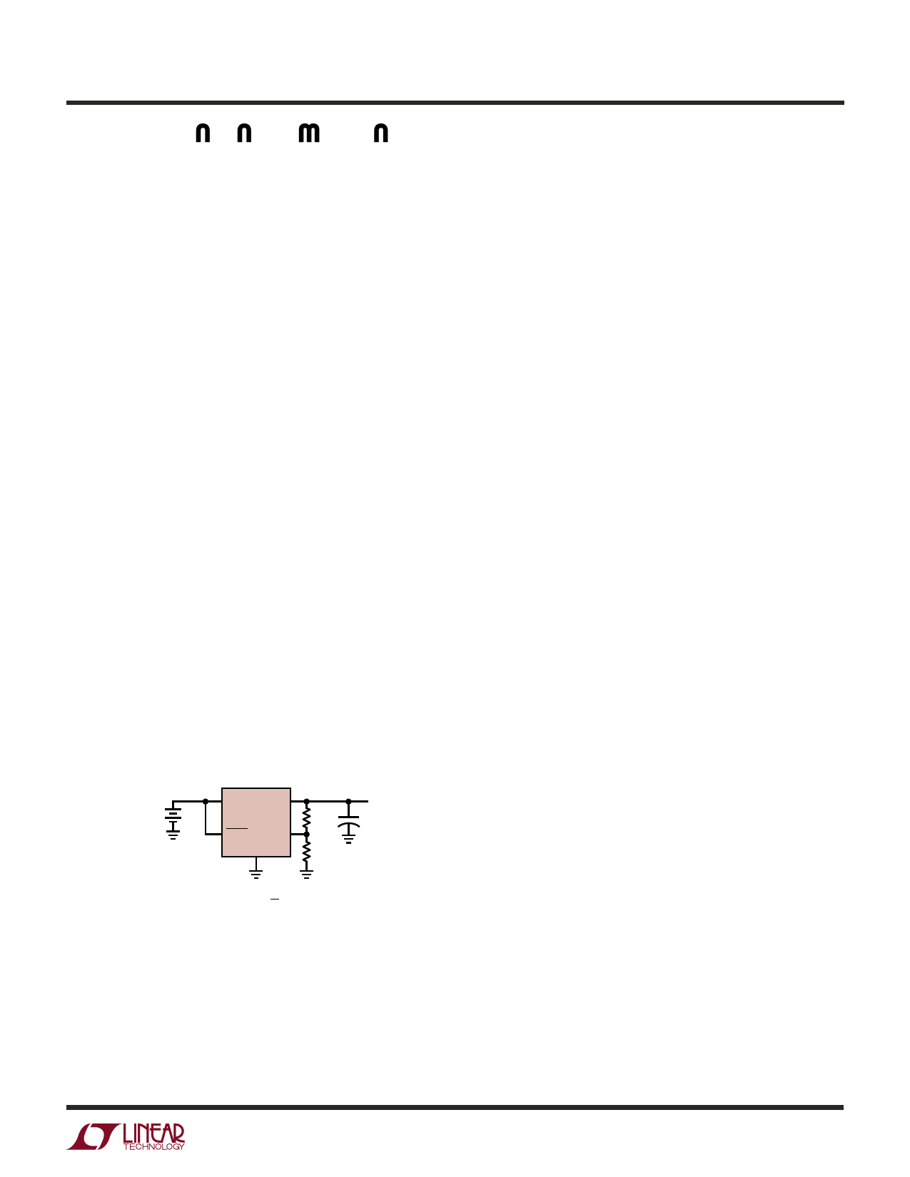
Adjustable Operation
The LT3021’s output voltage range is 0.2V to 9.5V. Figure
1 shows that the output voltage is set by the ratio of two
external resistors. The device regulates the output to
maintain the ADJ pin voltage at 200mV referenced to
ground. The current in R1 equals 200mV/R1 and the
current in R2 is the current in R1 minus the ADJ pin bias
current. The ADJ pin bias current of 20nA flows out of the
pin. Use the formula in Figure 1 to calculate output voltage.
An R1 value of 20k sets the resistor divider current to
10µA. Note that in shutdown the output is turned off and
the divider current is zero. Curves of ADJ Pin Voltage vs
Temperature and ADJ Pin Bias Current vs Temperature
appear in the Typical Performance Characteristics section.
VIN
IN
OUT
LT3021
+
R2
VOUT
SHDN ADJ
GND
R1
3021 F01
( ) VOUT = 200mV
1 + R2
R1
– IADJ (R2)
VADJ = 200mV
IADJ = 20nA AT 25°C
OUTPUT RANGE = 0.2V TO 9.5V
Figure 1. Adjustable Operation
Specifications for output voltages greater than 200mV are
proportional to the ratio of desired output voltage to
200mV; (VOUT/200mV). For example, load regulation for
an output current change of 1mA to 500mA is typically
0.4mV at VADJ = 200mV. At VOUT = 1.5V, load regulation is:
(1.5V/200mV) • (0.4mV) = 3mV
Output Capacitance and Transient Response
The LT3021’s design is stable with a wide range of output
capacitors, but is optimized for low ESR ceramic capaci-
tors. The output capacitor’s ESR affects stability, most
notably with small value capacitors. Use a minimum
output capacitor of 3.3µF with an ESR of 0.2Ω or less to
prevent oscillations. The LT3021 is a low voltage device,
and output load transient response is a function of output
capacitance. Larger values of output capacitance decrease
the peak deviations and provide improved transient re-
sponse for larger load current changes. For output capaci-
tor values greater than 22µF a small feedforward capacitor
with a value of 300pF across the upper divider resistor (R2
in Figure 1) is required. Under extremely low output
current conditions (ILOAD < 30µA) a low frequency small
signal oscillation (200Hz/8mVP-P at 1.2V output) can
occur. A minimum load of 100µA is recommended to
prevent this instability.
Give extra consideration to the use of ceramic capacitors.
Manufacturers make ceramic capacitors with a variety of
dielectrics, each with a different behavior across tempera-
ture and applied voltage. The most common dielectrics are
Z5U, Y5V, X5R and X7R. The Z5U and Y5V dielectrics
provide high C-V products in a small package at low cost,
but exhibit strong voltage and temperature coefficients.
The X5R and X7R dielectrics yield highly stable
characterisitics and are more suitable for use as the output
capacitor at fractionally increased cost. The X5R and X7R
dielectrics both exhibit excellent voltage coefficient char-
acteristics. The X7R type works over a larger temperature
range and exhibits better temperature stability whereas
X5R is less expensive and is available in higher values.
Figures 2 and 3 show voltage coefficient and temperature
coefficient comparisons between Y5V and X5R material.
Voltage and temperature coefficients are not the only
sources of problems. Some ceramic capacitors have a
piezoelectric response. A piezoelectric device generates
voltage across its terminals due to mechanical stress, simi-
lar to the way a piezoelectric accelerometer or microphone
works. For a ceramic capacitor, the stress can be induced
by vibrations in the system or thermal transients. The re-
sulting voltages produced can cause appreciable amounts
3021fa
9
Share Link: 