LC86E6560 データシートの表示(PDF) - SANYO -> Panasonic
部品番号
コンポーネント説明
一致するリスト
LC86E6560 Datasheet PDF : 21 Pages
| |||
LC86E6560
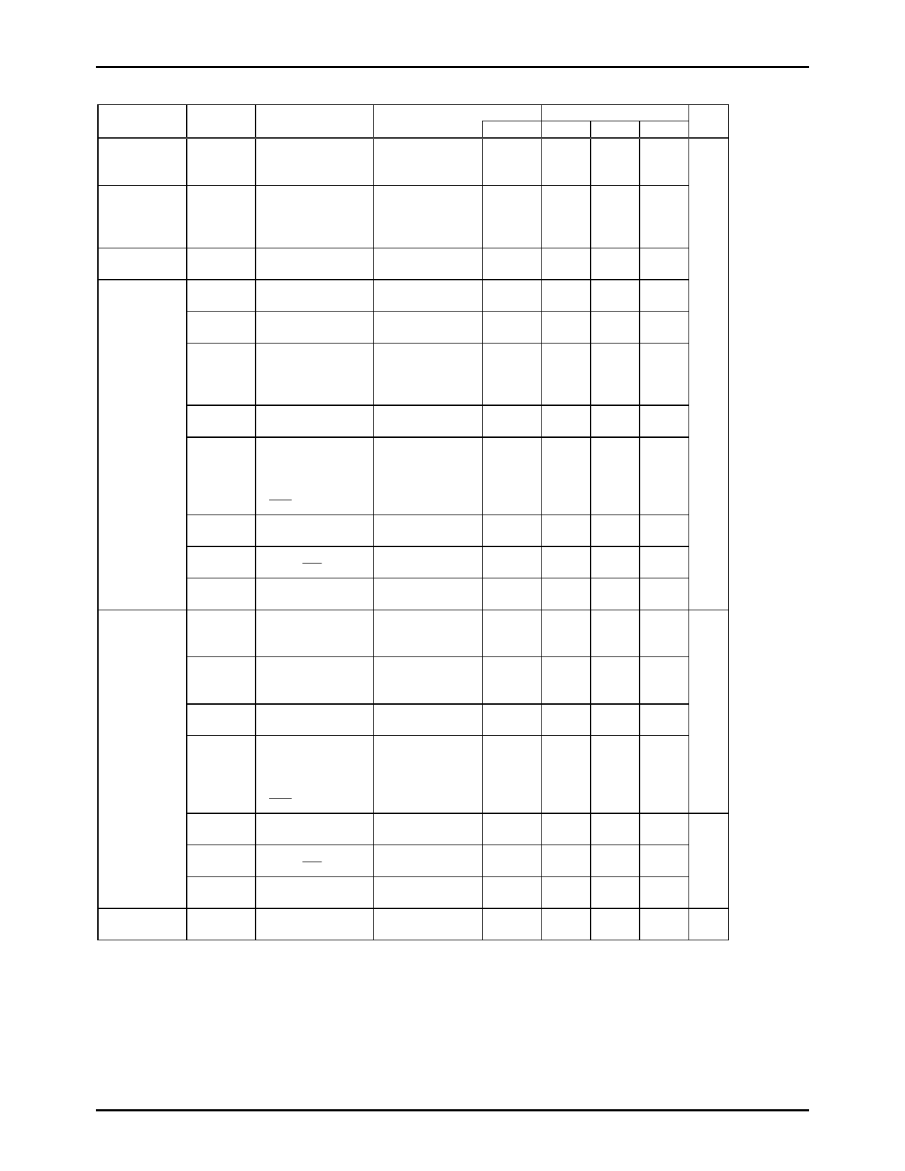
2. Recommended Operating Range at Ta=+10°C to +40°C, VSS1=VSS2=0V
Parameter
Symbol
Operating
supply voltage
range
Hold voltage
VDD(1)
VHD
Pins
VDD1=VDD2=
VDD3=VDD4
VDD1=VDD2
Pull-down
voltage
Input high
voltage
Input low
voltage
Operation
cycle time
VP
VIH(1)
VIH(2)
VIH(3)
VIH(4)
VIH(5)
VIH(6)
VIH(7)
VIH(8)
VIL(1)
VIL(2)
VIL(3)
VIL(4)
VIL(5)
VIL(6)
VIL(7)
tCYC
VP
Port 0 at CMOS
output option
Port 0 at N-ch
open drain output
•Port 1
•Ports 72, 73
•Port 3 at CMOS
output option
Port 3 at N-ch
open drain output
•Port 70
Port input
/interrupt
•Port 71
• RES
Port 70
Watchdog timer
•Port 8
•Ports P74 , 75
S16 to S51
Port 0 at
CMOS
output option
Port 0 at N-ch
open drain
output
•Ports 1, 3
•Ports 72, 73
•Port 70
Port input
/interrupt
•Port 71
• RES
Port 70
Watchdog timer
•Port 8
•Ports P74 , 75
S16 to S51
Conditions
0.98µs≤tCYC
≤400µs
Ratings
unit
VDD[V] min. typ. max.
4.5
6.0 V
RAMs and
2.0
registers hold
voltage at HOLD
mode.
4.5 - 6.0 -35
6.0
VDD
Output disable
Output disable
4.5 - 6.0 0.33VDD
+1.0
4.5 - 6.0 0.75VDD
VDD
13.5
Output disable
4.5 - 6.0 0.75VDD
VDD
Output disable
Tr. OFF
Output disable
4.5 - 6.0 0.75VDD
4.5 - 6.0 0.75VDD
13.5
VDD
Output disable
4.5 - 6.0 0.9VDD
Output disable
4.5 - 6.0 0.75VDD
Output P- channel
Tr. OFF
Output disable
4.5 - 6.0 0.33VDD
+1.0
4.5 - 6.0 VSS
Output disable
4.5 - 6.0 VSS
Output disable
Output disable
4.5 - 6.0 VSS
4.5 - 6.0 VSS
VDD
VDD
VDD
0.2VDD V
0.25VDD
0.25VDD
0.25VDD
Output disable
4.5 - 6.0 VSS
Output disable
4.5 - 6.0 VSS
Output P- channel 4.5 - 6.0 VP
Tr. OFF
4.5 - 6.0 0.98
(Continue)
0.8VDD V
-1.0
0.25VDD
0.2VDD
400 µs
No.6750-11/21
Share Link: 