LAG639 データシートの表示(PDF) - Mitsumi
部品番号
コンポーネント説明
一致するリスト
LAG639 Datasheet PDF : 8 Pages
| |||
MITSUMI
IC for Multifunction Telephones LAG639
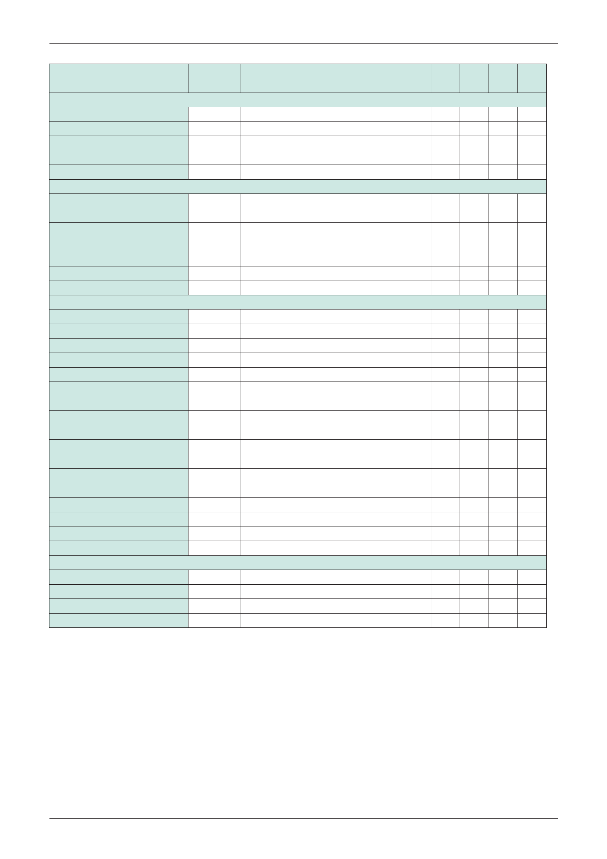
Item
Symbol
Beep sound generator unit
Beep sound frequency
Beep off switching point
Fb
Ibsw
Beep sound output 1
Vob1
Beep sound output 2
Watchdog timer unit
Vob2
Timer time
Tt
Output pulse width
TPW
Output voltage while on
Leakage output current while off
Transmission circuit unit
Transmission output voltage
Transmission waveform symmetry
Reception sensitivity
Noise resistance
Input IMP
Transmission delay time
VWON
IWOFF
Vto
Vtr
Vrs
Vrn
RIN3
Td1
Transmission delay time
Td2
Transmission delay time
Td3
Transmission delay time
Td4
Reception output H voltage VroH
Reception output L voltage VroL
Transmission waveform LOSS 1 Vtloss1
Transmission waveform LOSS 2 Vtloss2
General logic unit characteristics
H level input voltage
ViH
L level input voltage
ViL
H level input current
IiH
L level input current
IiL
Measurement
Measurement conditions Min.
circuit
1
0.85
1
Pin 9 input current
20
Pin 9 connected to GND through 4.7k
1
1.0
Amp output voltage
1
Pin 9 connected to GND through 47k 0.11
cf. watchdog timer
1
0.8
waveform diagram
cf. watchdog timer
0.45
1
waveform diagram
(1/2T)
T=beep sound period
1
1
1
Both pins 27 and 28
3.8
1
Vt1/Vt2
0.75
1
1.0
1
Level at which no errors are output 0.8
3
Both pins 7and 8
25
cf. transmit/receive
1
waveform diagrams
cf. transmit/receive
1
waveform diagrams
cf. transmit/receive
1
waveform diagrams
cf. transmit/receive
1
waveform diagrams
1
4
1
1
Vt=5V applied, power on 4.5
1
Vt=5V applied, power off 4.5
3
2.4
3
3
VIN=2.4V
3
VIN=0.4V
Typ.
1.0
35
1.4
0.16
1.0
4.2
1
1.2
36
0.5
0.4
1.2
1.5
Max. Units
1.15 kHz
48 µA
1.8 Vrms
0.22 Vrms
1.2 S
1.1
mS
(1T)
0.5 V
1 µA
4.6 VP-P
1.25
1.5 VP-P
VP-P
46 kΩ
µS
µS
µS
µS
V
0.5 V
VP-P
VP-P
V
0.8 V
10 µA
-300 µA
Share Link: 