L3G4200D データシートの表示(PDF) - STMicroelectronics
部品番号
コンポーネント説明
一致するリスト
L3G4200D Datasheet PDF : 24 Pages
| |||
Mechanical and electrical specifications
L3G4200D
2.3
2.3.1
Communication interface characteristics
SPI - serial peripheral interface
Subject to general operating conditions for Vdd and Top.
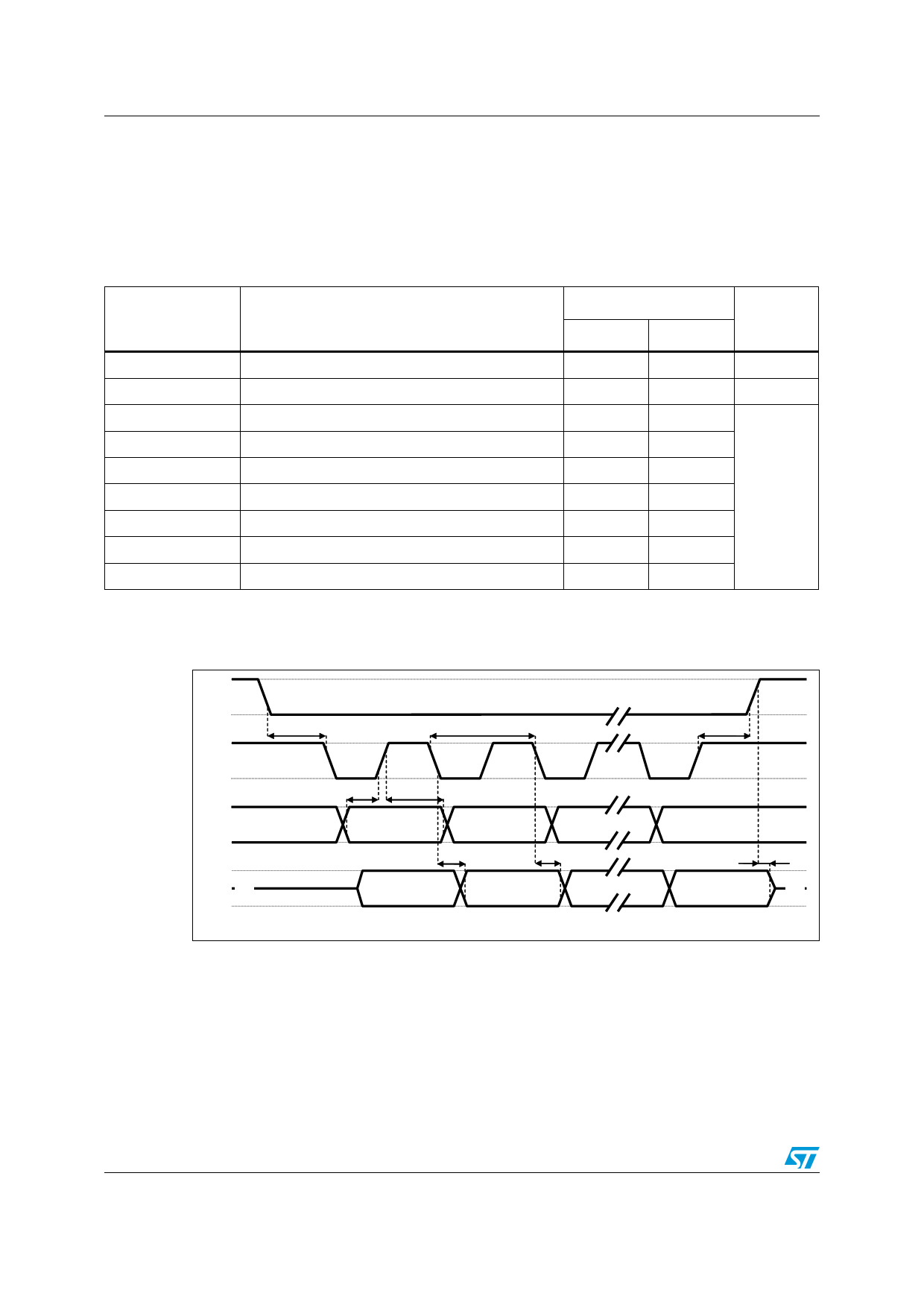
Table 6. SPI slave timing values
Symbol
Parameter
Value(1)
Min.
Max.
Unit
tc(SPC)
fc(SPC)
tsu(CS)
th(CS)
tsu(SI)
th(SI)
tv(SO)
th(SO)
tdis(SO)
SPI clock cycle
SPI clock frequency
CS setup time
CS hold time
SDI input setup time
SDI input hold time
SDO valid output time
SDO output hold time
SDO output disable time
100
ns
10
MHz
5
8
5
15
ns
50
6
50
1. Values are guaranteed at 10 MHz clock frequency for SPI with both 4 and 3 wires, based on characterization results, not
tested in production.
Figure 4. SPI slave timing diagram (2)
#3� �
30#� �
TSU#3 �
3$)� �
3$/� �
TC30# �
TSU3) �
TH3) �
-3"�).�
TV3/ �
-3"�/54�
TH3/ �
�
TH#3 �
�
,3"�).�
�
TDIS3/ �
,3"�/54�
�
2. Measurement points are done at 0.2·Vdd_IO and 0.8·Vdd_IO, for both Input and Output port
!-V
10/24
Doc ID 17116 Rev 1
Share Link: 