ISL84582 データシートの表示(PDF) - Intersil
部品番号
コンポーネント説明
一致するリスト
ISL84582 Datasheet PDF : 14 Pages
| |||
ISL84582
Electrical Specifications: 3.3V Supply Test Conditions: V+ = +3V to +3.6V, V- = GND = 0V, VINH = 2.4V, VINL = 0.8V (Note 3) Unless
Otherwise Specified. (Continued)
PARAMETER
TEST CONDITIONS
TEMP
MIN
MAX
(°C) (Notes 4, 10) TYP (Notes 4, 10) UNITS
Break-Before-Make Time, tBBM V+ = 3.6V, VNO or VNC = 1.5V, RL = 300Ω, CL = 35pF, Full
3
13
-
ns
VIN = 0 to 3V (see Figure 3, Note 9)
Charge Injection, Q
CL = 1.0nF, VG = 0V, RG = 0Ω, (See Figure 2, Note 9) 25
-
0.3
1
pC
OFF-Isolation
Crosstalk, (Note 8)
RL = 50Ω, CL = 15pF, f = 100kHz,
25
-
92
-
dB
VNO or VNC = 1VRMS (see Figures 4, 6 and 19)
25
-
≤110
-
dB
All Hostile Crosstalk, (Note 8)
25
-
-105
-
dB
POWER SUPPLY CHARACTERISTICS
Power Supply Range
Full
3.0
-
3.6
V
Positive Supply Current, I+
V+ = 3.6V, V- = 0V, VINH, VADD = 0V or V+,
Switch On or Off, (Note 9)
Full
-1
-
1
µA
NOTES:
3. VIN = Input logic voltage to configure the device in a given state.
4. The algebraic convention, whereby the most negative value is a minimum and the most positive a maximum, is used in this data sheet.
5. ΔrON = rON (MAX) - rON (MIN).
6. Flatness is defined as the difference between maximum and minimum value of on-resistance over the specified analog signal range.
7. Leakage parameter is 100% tested at high temp, and guaranteed by correlation at +25°C.
8. Between any two switches.
9. Limits established by characterization and are not production tested.
10. Parameters with MIN and/or MAX limits are 100% tested at +25°C, unless otherwise specified. Temperature limits established by
characterization and are not production tested.
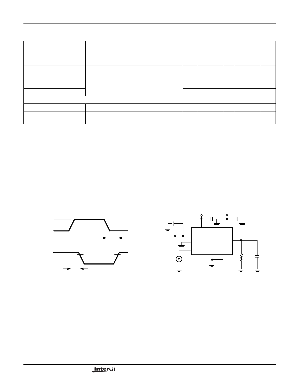
Test Circuits and Waveforms
3V
LOGIC
INPUT
0V
50%
tON
tr < 20ns
tf < 20ns
VNO0
SWITCH
OUTPUT 0V
tOFF
90% VOUT
90%
Logic input waveform is inverted for switches that have the opposite
logic sense.
FIGURE 1A. INHIBIT tON/tOFF MEASUREMENT POINTS
C
V+
LOGIC
INPUT
V+
C
V-
C
NO0x
NO1x-NO3x
ISL84582
COMx
INH
GND ADDA-B
VOUT
RL
300Ω
CL
35pF
Repeat test for other switches. CL includes fixture and stray
capacitance.
VOUT
=
V(NO or NC)
-----------R-----L------------
RL + r(ON)
FIGURE 1B. INHIBIT tON/tOFF TEST CIRCUIT
7
FN6213.3
May 6, 2009
Share Link: 