84052IAZ データシートの表示(PDF) - Intersil
部品番号
コンポーネント説明
一致するリスト
84052IAZ Datasheet PDF : 18 Pages
| |||
ISL84051, ISL84052, ISL84053
Detailed Description
The ISL84051, ISL84052, ISL84053 analog switches offer
precise switching capability from a bipolar ±2V to ±6V or a
single 2V to 12V supply with low on-resistance (60Ω) and
high speed operation (tON = 50ns, tOFF = 40ns). The devices
are especially well suited to portable battery powered
equipment thanks to the low operating supply voltage (2V),
low power consumption (3μW), low leakage currents (5nA
max). High frequency applications also benefit from the wide
bandwidth, and the very high off isolation and crosstalk
rejection.
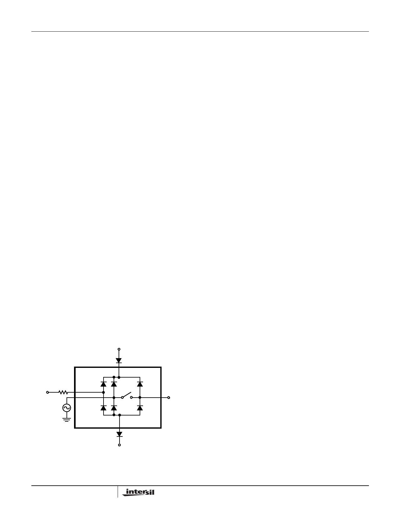
Supply Sequencing And Overvoltage Protection
With any CMOS device, proper power supply sequencing is
required to protect the device from excessive input currents
which might permanently damage the IC. All I/O pins contain
ESD protection diodes from the pin to V+ and to V- (see
Figure 8). To prevent forward biasing these diodes, V+ and
V- must be applied before any input signals, and input signal
voltages must remain between V+ and V-. If these conditions
cannot be guaranteed, then one of the following two
protection methods should be employed.
Logic inputs can easily be protected by adding a 1kΩ
resistor in series with the input (see Figure 8). The resistor
limits the input current below the threshold that produces
permanent damage, and the sub-microamp input current
produces an insignificant voltage drop during normal
operation.
This method is not applicable for the signal path inputs.
Adding a series resistor to the switch input defeats the
purpose of using a low rON switch, so two small signal
diodes can be added in series with the supply pins to provide
overvoltage protection for all pins (see Figure 8). These
additional diodes limit the analog signal from 1V below V+ to
1V above V-. The low leakage current performance is
unaffected by this approach, but the switch resistance may
increase, especially at low supply voltages.
OPTIONAL
PROTECTION
RESISTOR
FOR LOGIC
INPUTS
OPTIONAL PROTECTION
DIODE
V+
1kΩ LOGIC
VNO OR NC
VCOM
V-
OPTIONAL PROTECTION
DIODE
FIGURE 8. INPUT OVERVOLTAGE PROTECTION
Power-Supply Considerations
The ISL8405x construction is typical of most CMOS analog
switches, in that they have three supply pins: V+, V-, and
GND. V+ and V- drive the internal CMOS switches and set
their analog voltage limits, so there are no connections
between the analog signal path and GND. Unlike switches
with a 13V maximum supply voltage, the ISL8405x 15V
maximum supply voltage provides plenty of room for the
10% tolerance of 12V supplies (±6V or 12V single supply),
as well as room for overshoot and noise spikes.
This family of switches performs equally well when operated
with bipolar or single voltage supplies. The minimum
recommended supply voltage is 2V or ±2V. It is important to
note that the input signal range, switching times, and
ON-resistance degrade at lower supply voltages. Refer to
the “Electrical Specification” tables beginning on page 4 and
“Typical Performance Curves” beginning on page 13 for
details.
V+ and GND power the internal logic (thus setting the digital
switching point) and level shifters. The level shifters convert
the logic levels to switched V+ and V- signals to drive the
analog switch gate terminals.
Logic-Level Thresholds
V+ and GND power the internal logic stages, so V- has no
affect on logic thresholds. This switch family is TTL
compatible (0.8V and 2.4V) over a V+ supply range of 2.7V
to 10V. At 12V the VIH level is about 3.5V. This is still below
the CMOS guaranteed high output minimum level of 4V, but
noise margin is reduced. For best results with a 12V supply,
use a logic family that provides a VOH greater than 4V.
The digital input stages draw supply current whenever the
digital input voltage is not at one of the supply rails. Driving
the digital input signals from GND to V+ with a fast transition
time minimizes power dissipation.
High-Frequency Performance
In 50Ω systems, signal response is reasonably flat even past
100MHz (see Figure 17). Figure 17 also illustrates that the
frequency response is very consistent over varying analog
signal levels.
An OFF switch acts like a capacitor and passes higher
frequencies with less attenuation, resulting in signal feed
through from a switch’s input to its output. Off isolation is the
resistance to this feed through, while crosstalk indicates the
amount of feed through from one switch to another.
Figure 18 details the high off isolation and crosstalk rejection
provided by this family. At 10MHz, off isolation is about 55dB
in 50Ω systems, decreasing approximately 20dB per decade
as frequency increases. Higher load impedances decrease
off isolation and crosstalk rejection due to the voltage divider
action of the switch OFF impedance and the load
impedance.
12
FN6047.8
October 2, 2007
Share Link: 