ISL84052IA-T(2003) データシートの表示(PDF) - Intersil
部品番号
コンポーネント説明
一致するリスト
ISL84052IA-T
(Rev.:2003)
(Rev.:2003)
Intersil

ISL84052IA-T Datasheet PDF : 17 Pages
| |||
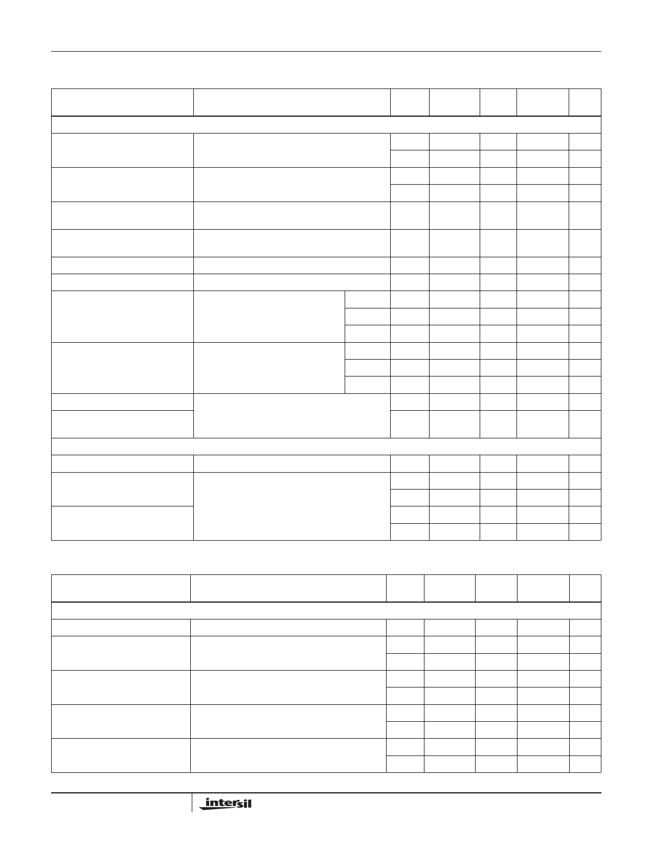
ISL84051, ISL84052, ISL84053
Electrical Specifications: ±5V Supply Test Conditions: VSUPPLY = ±4.5V to ±5.5V, GND = 0V, VINH = 2.4V, VINL = 0.8V (Note 4),
Unless Otherwise Specified (Continued)
PARAMETER
TEST CONDITIONS
TEMP (NOTE 5)
(NOTE 5)
(oC)
MIN
TYP
MAX UNITS
DYNAMIC CHARACTERISTICS
Inhibit Turn-ON Time, tON
VS = ±4.5V, VNO or VNC = ±3V, RL = 300Ω,
CL = 35pF, VIN = 0 to 3, (See Figure 1)
25
-
Full
-
50
175
ns
-
225
ns
Inhibit Turn-OFF Time, tOFF
VS = ±4.5V, VNO or VNC = ±3V, RL = 300Ω,
CL = 35pF, VIN = 0 to 3, (See Figure 1)
25
-
Full
-
40
150
ns
-
200
ns
Address Transition Time, tTRANS
VS = ±4.5V, VNO or VNC = ±3V, RL = 300Ω,
CL = 35pF, VIN = 0 to 3, (See Figure 1)
25
-
Break-Before-Make Time, tBBM
VS = ±5.5V, VNO or VNC = 3V, RL = 300Ω,
CL = 35pF, VIN = 0 to 3V, (See Figure 3)
25
2
Charge Injection, Q
CL = 1.0nF, VG = 0V, RG = 0Ω, (See Figure 2)
25
-
NO/NC OFF Capacitance, COFF
f = 1MHz, VNO or VNC = VCOM = 0V, (See Figure 7) 25
-
COM OFF Capacitance, COFF
f = 1MHz, VNO or VNC = VCOM = 0V, ISL84051
25
-
(See Figure 7)
ISL84052 25
-
75
250
ns
10
-
ns
2
10
pC
3
-
pF
21
-
pF
12
-
pF
ISL84053 25
-
9
-
pF
COM ON Capacitance, CCOM(ON) f = 1MHz, VNO or VNC = VCOM = 0V, ISL84051
25
-
26
-
pF
(See Figure 7)
ISL84052 25
-
18
-
pF
ISL84053 25
-
14
-
pF
OFF Isolation
Crosstalk, (Note 9) (ISL84052,
ISL84053 only)
RL = 50Ω, CL = 15pF, f = 100kHz,
VNO or VNC = 1VRMS, (See Figures 4 and 6)
25
-
<90
-
dB
25
-
<-90
-
dB
POWER SUPPLY CHARACTERISTICS
Power Supply Range
Full
±2
-
±6
V
Positive Supply Current, I+
VS = ±5.5V, VINH, VADD = 0V or V+, Switch On or
25
-1
0.1
1
µA
Off
Full
-10
-
10
µA
Negative Supply Current, I-
25
-1
0.1
1
µA
Full
-10
-
10
µA
NOTES:
4. VIN = Input voltage to perform proper function.
5. The algebraic convention, whereby the most negative value is a minimum and the most positive a maximum, is used in this data sheet.
6. ∆RON = RON (MAX) - RON (MIN).
7. Flatness is defined as the difference between maximum and minimum value of on-resistance over the specified analog signal range.
8. Leakage parameter is 100% tested at high temp, and guaranteed by correlation at 25oC.
9. Between any two switches.
5
Share Link: