IDT7132 データシートの表示(PDF) - Integrated Device Technology
部品番号
コンポーネント説明
一致するリスト
IDT7132 Datasheet PDF : 16 Pages
| |||
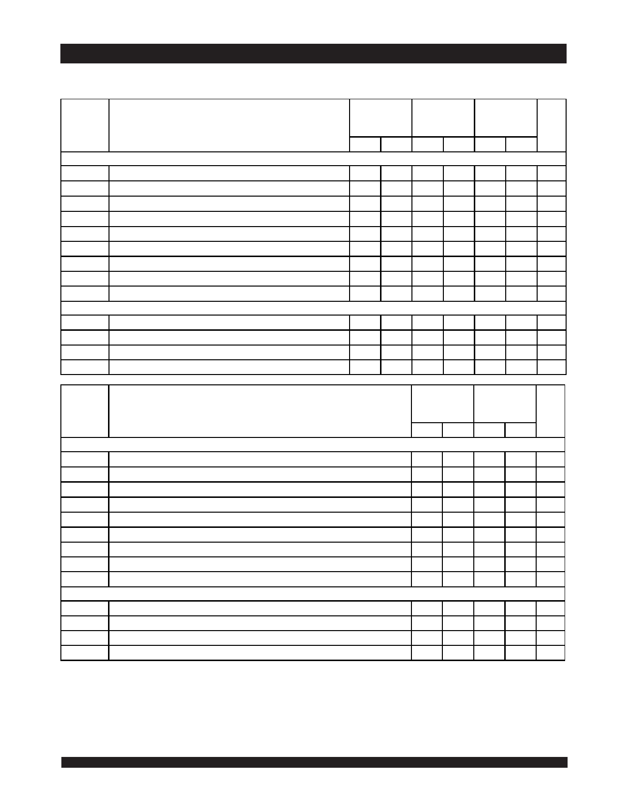
IDT7132SA/LA and IDT 7142SA/LA
High Speed 2K x 8 Dual Port Static RAM
Military, Industrial and Commercial Temperature Ranges
AC Electrical Characteristics Over the
Operating Temperature and Supply Voltage Range(7,8)
7132X20(1)
7142X20(1)
Com'l Only
7132X25(2)
7142X25(2)
Com'l, Ind
& Military
7132X35
7142X35
Com'l &
Military
Symbol
BUSY Timing (For Master IDT7132 Only)
Parameter
Min. Max. Min. Max. Min. Max. Unit
tBAA
BUSY Access Time from Address
____
20
____
20
____
20
ns
tBDA
BUSY Disable Time from Address
____
20
____
20
____
20
ns
tBAC
BUSY Access Time from Chip Enable
____
20
____
20
____
20
ns
tBDC
BUSY Disable Time from Chip Enable
tWDD
Write Pulse to Data Delay(2)
tWH
Write Hold After BUSY(6)
tDDD
Write Data Valid to Read Data Delay(2)
tAPS
Arbitration Priority Set-up Time(3)
____
20
____
20
____
20
ns
____
50
____
50
____
60
ns
12
____
15
____
20
____
ns
____
35
____
35
____
35
ns
5
____
5
____
5
____
ns
tBDD
BUSY Disable to Valid Data(4)
BUSY Timing (For Slave IDT7142 Only)
tWB
Write to BUSY Input(5)
tWH
Write Hold After BUSY(6)
tWDD
Write Pulse to Data Delay(2)
tDDD
Write Data Valid to Read Data Delay(2)
____
25
____
35
____
35
ns
0
____
0
____
0
____
ns
12
____
15
____
20
____
ns
____
40
____
50
____
60
ns
____
30
____
35
____
35
ns
7132X55
7142X55
Com'l &
Military
7132X100
7142X100
Com'l &
Military
2692 tbl 11a
Symbol
BUSY Timing (For Master IDT7132 Only)
Parameter
Min. Max. Min. Max. Unit
tBAA
BUSY Access Time from Address
tBDA
BUSY Disable Time from Address
____
30
____
50
ns
____
30
____
50
ns
tBAC
BUSY Access Time from Chip Enable
____
30
____
50
ns
tBDC
BUSY Disable Time from Chip Enable
tWDD
Write Pulse to Data Delay(2)
tWH
Write Hold After BUSY(6)
tDDD
Write Data Valid to Read Data Delay(2)
tAPS
Arbitration Priority Set-up Time(3)
____
30
____
50
ns
____
80
____
120
ns
20
____
20
____
ns
____
55
____
100
ns
5
____
5
____
ns
tBDD
BUSY Disable to Valid Data(4)
BUSY Timing (For Slave IDT7142 Only)
tWB
Write to BUSY Input(5)
tWH
Write Hold After BUSY(6)
tWDD
Write Pulse to Data Delay(2)
tDDD
Write Data Valid to Read Data Delay(2)
____
50
____
65
ns
0
____
0
____
ns
20
____
20
____
ns
____
80
____
120
ns
____
55
____
100
ns
NOTES:
1. PLCC package only.
2. Port-to-port delay through RAM cells from the writing port to the reading port, refer to “Timing Waveform of Write with Port -to-Port Read and BUSY.”
3. To ensure that the earlier of the two ports wins.
4. tBDD is a calculated parameter and is the greater of 0, tWDD – tWP (actual) or tDDD – tDW (actual).
5. To ensure that a write cycle is inhibited on port "B" during contention on port "A".
6. To ensure that a write cycle is completed on port "B" after contention on port "A".
7. 'X' in part numbers indicates power rating (SA or LA).
8. Industrial temperature: for specific speeds, packages and powers contact your sales office.
2692 tbl 11b
61.412
Share Link: 