ICS94229 データシートの表示(PDF) - Integrated Circuit Systems
部品番号
コンポーネント説明
一致するリスト
ICS94229 Datasheet PDF : 17 Pages
| |||
ICS94229
Advance Information
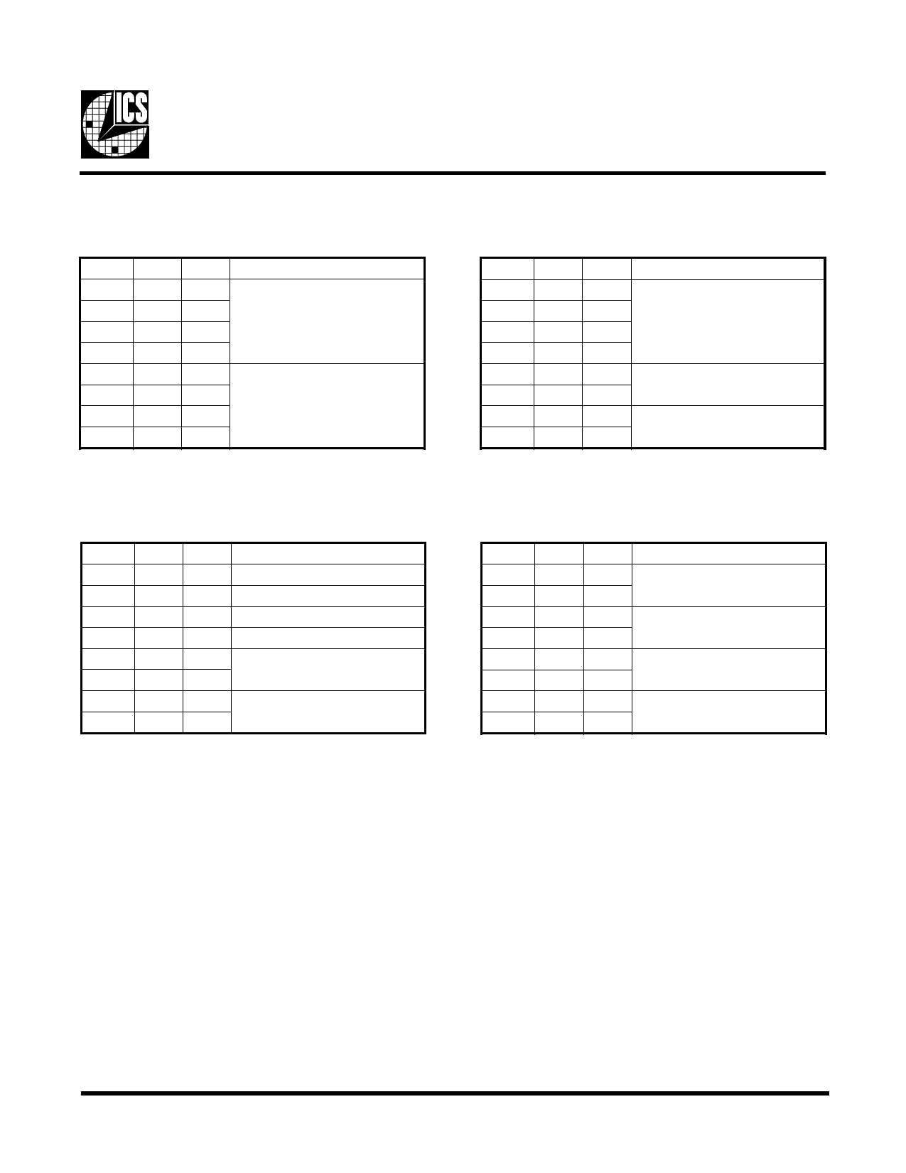
Byte 13: Output Skew Control Register
(1= enable, 0 = disable)
BIT
Bit 7
Bit 6
Bit 5
Bit 4
Bit 3
Bit 2
Bit 1
Bit 0
PIN#
-
-
-
-
-
-
-
-
PWD
0
0
0
0
0
0
0
0
DESCRIPTION
CPUCLKC0/T0 Skew Control
CPUCLKC_CST/C Skew Control
Byte 14: Output Skew Control Register
(1= enable, 0 = disable)
BIT
Bit 7
Bit 6
Bit 5
Bit 4
Bit 3
Bit 2
Bit 1
Bit 0
PIN#
-
-
-
-
-
-
-
-
PWD
DESCRIPTION
0
0
PCICLK(8:0) Skew Control
1
0
0
AGP(2:0) Skew Control
0
0
PCICLK9_E: Slew Rate Control
0
Byte 15: Output Rise/Fall Time Select Register
(1= enable, 0 = disable)
BIT
Bit 7
Bit 6
Bit 5
Bit 4
Bit 3
Bit 2
Bit 1
Bit 0
PIN#
-
-
-
-
-
-
-
-
PWD
DESCRIPTION
0 CPUCLKT0
0 CPUCLKC0
0 CPUCLKT_CST
0 CPUCLKC_CSC
1
AGP(2:0): Slew Rate Control
0
0
REF(2:0): Slew Rate Control
0
Byte 16: Output Rise/Fall Time Select Register
(1= enable, 0 = disable)
BIT
Bit 7
Bit 6
Bit 5
Bit 4
Bit 3
Bit 2
Bit 1
Bit 0
PIN#
-
-
-
-
-
-
-
-
PWD
0
0
1
0
0
0
0
0
DESCRIPTION
PCICLK(3:0): Slew Rate Control
PCICLK(8:4): Slew Rate Control
48MHz: Slew Rate Control
24_48MHz: Slew Rate Control
Third party brands and names are the property of their respective owners.
9
Share Link: 