HY628100B データシートの表示(PDF) - Hynix Semiconductor
部品番号
コンポーネント説明
一致するリスト
HY628100B Datasheet PDF : 10 Pages
| |||
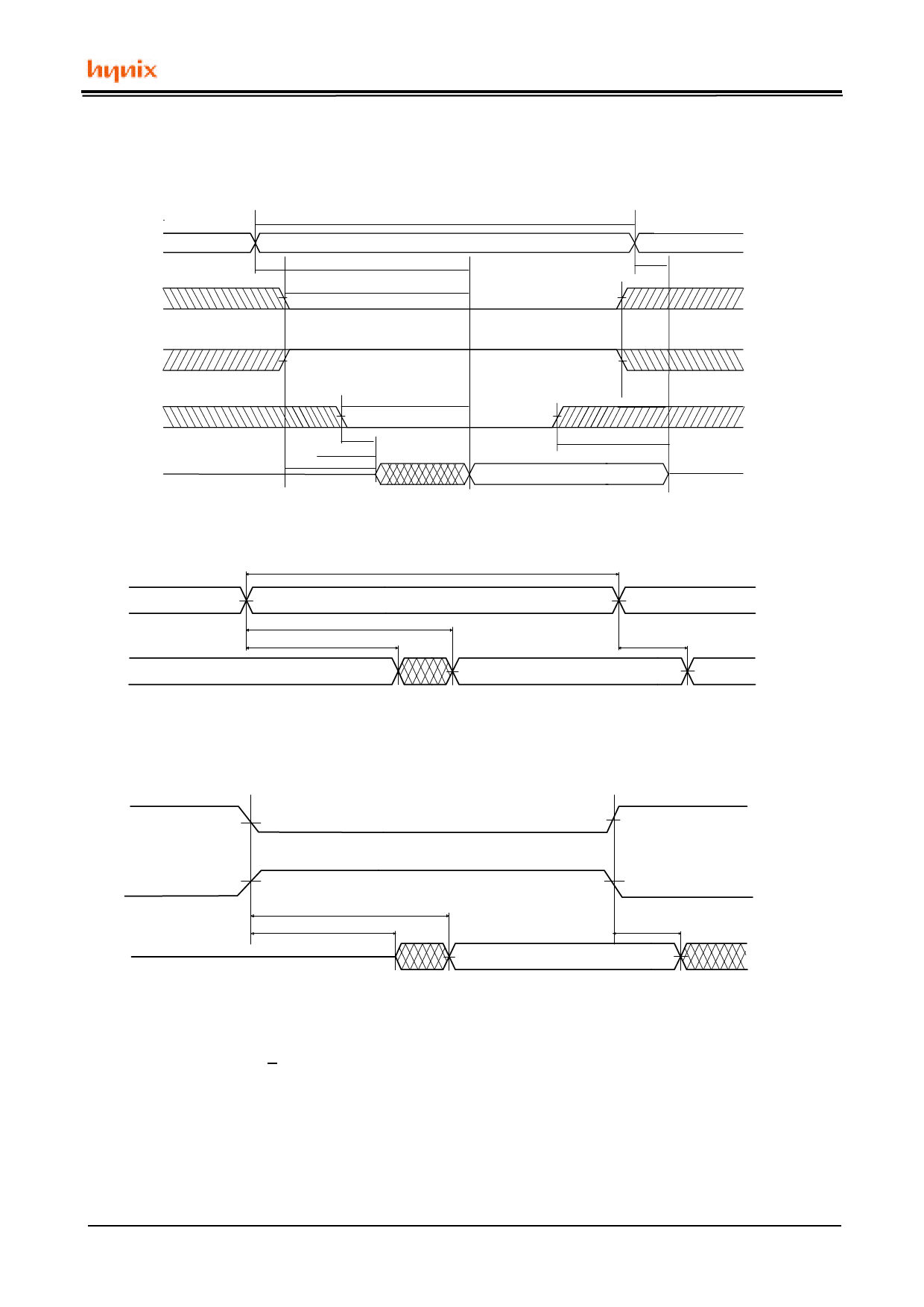
TIMING DIAGRAM
READ CYCLE 1(Note 1,4)
ADDR
/CS1
tRC
tAA
tACS
CS2
/OE
Data
Out
High-Z
tOE
tCLZ(3)
tOLZ(3)
READ CYCLE 2(Note 1,2,4)
tRC
ADDR
Data
Out
tAA
tOH
Previous Data
HY628100B Series
tOH
tCHZ(3)
tOHZ(3)
Data Valid
tOH
Data Valid
READ CYCLE 3(Note 1,2,4)
/CS1
CS2
Data
Out
tACS
tCLZ(3)
Data Valid
tCHZ(3)
Notes:
1. A read occurs during the overlap of a low /OE, a high /WE, a low /CS1 and a high CS2.
2. /OE = VIL
3. Transition is measured + 200mV from steady state voltage.
This parameter is sampled and not 100% tested.
4. /CS1 in high for the standby, low for active
CS2 in low for the standby, high for active
Rev 12 / Apr.2001
5
Share Link: 