HSP45116GM-15883 データシートの表示(PDF) - Intersil
部品番号
コンポーネント説明
一致するリスト
HSP45116GM-15883 Datasheet PDF : 18 Pages
| |||
HSP45116
Functional Description
The Numerically Controlled Oscillator/Modulator (NCOM)
produces a digital complex sinusoid waveform whose
amplitude, phase and frequency are controlled by a set of
input command words. When used as a Numerically
Controlled Oscillator (NCO), it generates 16-bit sine and
cosine vectors at a maximum sample rate of 33MHz. The
NCOM can be preprogrammed to produce a constant (CW)
sine and cosine output for Direct Digital Synthesis (DDS)
applications. Alternatively, the phase and frequency inputs
can be updated in real time to produce a FM, PSK, FSK, or
MSK modulated waveform. The Complex Multiplier/
Accumulator (CMAC) can be used to multiply this waveform
by an input signal for AM and QAM signals. By stepping the
phase input, the output of the ROM becomes an FFT twiddle
factor; when data is input to the Vector Inputs (see Block
Diagram), the NCOM calculates an FFT butterfly.
As shown in the Block Diagram, the NCOM consists of three
parts: Phase and Frequency Control Section (PFCS),
Sine/Cosine Generator, and CMAC. The PFCS stores the
phase and frequency inputs and uses them to calculate the
phase angle of a rotating complex vector. The Sine/Cosine
Generator performs a lookup on this phase and outputs the
appropriate values for the sine and cosine. The sine and
cosine form one set of inputs to the CMAC, which multiplies
them by the input vector to form the modulated output.
Phase and Frequency Control Section
The phase and frequency of the internally generated sine
and cosine are controlled by the PFCS (Block Diagram). The
PFCS generates a 32-bit word that represents the current
phase of the sine and cosine waves being generated; the
Sine/ Cosine Argument. Stepping this phase angle from 0
through full scale (232 - 1) corresponds to the phase angle of
a sinusoid starting at 0o and advancing around the unit circle
counterclockwise. The PFCS automatically increments the
phase by a preprogrammed amount on every rising edge of
the external clock. The value of the phase step (which is the
sum of the Center and Offset Frequency Registers) is:
Phase Step = S-C----i-lg-o--n-c---ak---l--F-F---r-r-e-e--q-q--u-u---e-e--n-n---cc---yy-- × 232
The PFCS is divided into two sections: the Phase
Accumulator uses the data on C0-15 to compute the phase
angle that is the input to the Sine/Cosine Section
(Sine/Cosine Argument); the Time Accumulator supplies a
pulse to mark the passage of a preprogrammed period of
time.
The Phase Accumulator and Time Accumulator work on the
same principle: a 32-bit word is added to the contents of a
32-bit accumulator register every clock cycle; when the sum
causes the adder to overflow, the accumulation continues
with the 32 bits of the adder going into the accumulator
register. The overflow bit is used as an output to indicate the
timing of the accumulation overflows. In the Time
Accumulator, the overflow bit generates TICO, the Time
Accumulator carry out (which is the only output of the Time
Accumulator). In the Phase Accumulator, the overflow is
inverted to generate the Phase Accumulator Carry Out,
PACO.
The output of the Phase Accumulator goes to the Phase
Adder, which adds an offset to the top 16 bits of the phase.
This 32-bit number forms the argument of the sine and
cosine, which is passed to the Sine/Cosine Generator.
Both accumulators are loaded 16 bits at a time over the
C0-15 bus. Data on C0-15 is loaded into one of the three
input registers when CS and WR are low. The data in the
Most Significant Input Register and Least Significant Input
Register forms a 32-bit word that is the input to the Center
Frequency Register, Offset Frequency Register and Time
Accumulator. These registers are loaded by enabling the
proper register enable signal; for example, to load the Center
Frequency Register, the data is loaded into the LS and MS
Input Registers, and ENCFREG is set to zero; the next rising
edge of CLK will pass the registered version of ENCFREG,
R.ENCFREG, to the clock enable of the Center Frequency
Register; this register then gets loaded on the following
rising edge of CLK. The contents of the Input Registers will
be continuously loaded into the Center Frequency Register
as long as R.ENCFREG is low.
The Phase Register is loaded in a similar manner. Assuming
PMSEL is high, the contents of the Phase Input Register is
loaded into the Phase Register on every rising clock edge
that R.ENPHREG is low. If PMSEL is low, MOD0-1 supply
the two most significant bits into the Phase Register (MOD1
is the MSB) and the least significant 14 bits are loaded with
0. MOD0-1 are used to generate a Quad Phase Shift Keying
(QPSK) signal (Table 2).
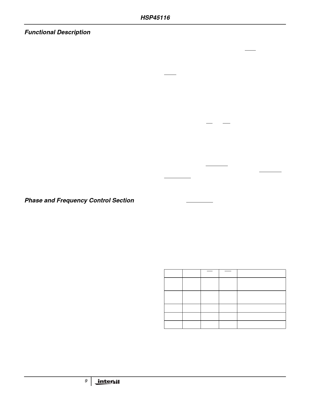
TABLE 1. AD0-1 DECODING
AD1 AD0
CS
WR
FUNCTION
0
0
0
↑ Load least significant bits
of frequency input.
0
1
0
↑ Load most significant bits
of frequency input.
1
0
0
↑ Load phase register.
1
1
X
X Reserved.
X
X
1
X No Operation.
The Phase Accumulator consists of registers and adders
that compute the value of the current phase at every clock. It
has three inputs: Center Frequency, which corresponds to
the carrier frequency of a signal; Offset Frequency, which is
the deviation from the Center Frequency; and Phase, which
is a 16-bit number that is added to the current phase for PSK
9
Share Link: 