HIP1011A データシートの表示(PDF) - Intersil
部品番号
コンポーネント説明
一致するリスト
HIP1011A Datasheet PDF : 11 Pages
| |||
HIP1011A
HIP1011A PCI Hot Plug Controller
Key Feature Description and Operation
A drop-in alternative to the widely used HIP1011, the
HIP1011A additionally features an adjustable delay time to
fault reporting and latch-off of the MOSFET switches. During
an over current condition (OC) on any output, or an under
voltage (UV) condition on the +5V, +3.3V or +12V outputs, a
LOW (0V) is presented on the FLTN output and all
MOSFETs are latched-off. A programmable delay time from
an OC or UV event to the FLTN signal going LOW and
MOSFET latch-off can be designed into the system by a
single capacitor from the FLTN pin to ground. The addition of
an increasingly larger capacitor value on the FLTN pin
increases the time from the OC or UV occurrence to the start
of the FLTN high to low transition. The capacitor also slows
the falling ramp thus delaying reaching the FLTN latch
threshold of ~2.4V. Once the FLTN latch voltage threshold is
reached the HIP1011A then simultaneously shuts down all
four supplies. This added feature enables the HIP1011A to
ignore both transient UV and OC events to the extent of a
single capacitor value in the system design. This feature also
may allow the system OS to complete housekeeping
activities in preparation for a possible unplanned shutdown
of the affected card by receiving an early warning signal from
the HIP1011A.
Customizing and Optimizing Circuit Performance
and Functionality
HOW ADJUSTABLE IS THE FAULT REPORTING DELAY
AND TIME TO POWER SUPPLY LATCH-OFF?
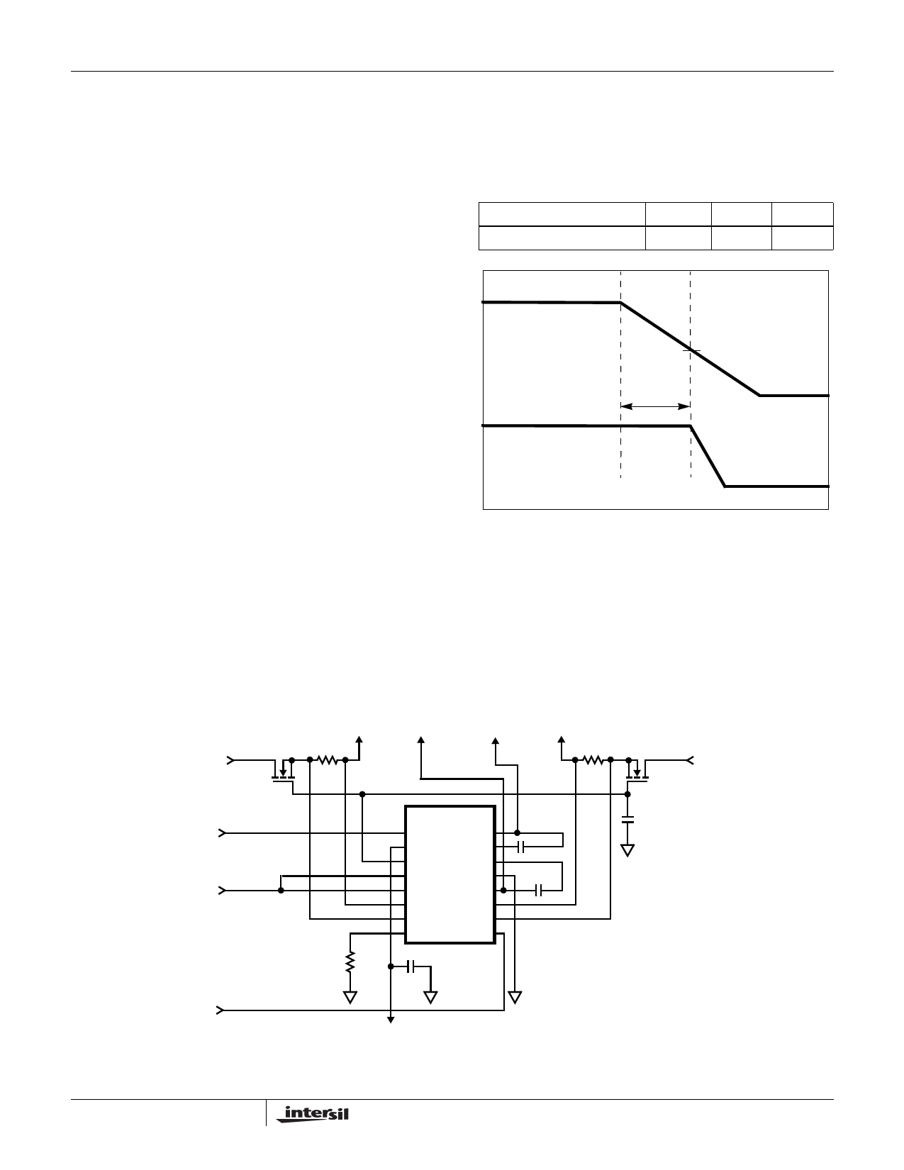
Figure 12 illustrates the relationship between the FLTN
signal and the gate drive outputs. Duration a, indicates the
time between FLTN starting to transition from High to Low,
3.3V INPUT
3.3V
7.6A OUT
5mΩ 1%
12V
0.5A OUT
(indicating a fault has occurred) and the start of the gate
drive outputs latching off. The latch-off is initiated by the
falling FLTN signal reaching the output latch threshold
voltage, VFLTN, TH. Table 1 illustrates the effect of the FLTN
capacitor on the response time.
TABLE 1. RESPONSE TIME TABLE
3V5VG Response a
0.001µF
0.85µs
0.1µF
37µs
10µF
3.8ms
VFLTN, TH
FLTN
a
3V5VG
T1
T2
FIGURE 12. TIMING DIAGRAM
CAN THE HIP1011A BE USED ON A CompactPCI
BOARD?
Yes, the HIP1011A can be used on a CompactPCI card
application. See Technical Brief TB358.
-12V
0.1A OUT
5V
5A OUT
5mΩ 1%
5V INPUT
-12V INPUT
12V INPUT
6.04kΩ
1%
HIP1011A
M12VIN M12VO
FLTN M12VG
3V5VG 12VG
VCC
12VIN
GND
12VO
3VISEN 5VISEN
3VS
5VS
OCSET PWRON
(SEE TABLE 1)
0.033µF
0.033µF
POWER CONTROL INPUT
NOTE:
3. All capacitors are ±±10%.
FAULT OUTPUT (ACTIVE LOW)
FIGURE 11. HIP1011A TYPICAL APPLICATION
8
0.033µF
FN4631.5
November 16, 2004
Share Link: 