HFA3824A データシートの表示(PDF) - Intersil
部品番号
コンポーネント説明
一致するリスト
HFA3824A Datasheet PDF : 40 Pages
| |||
HFA3824A
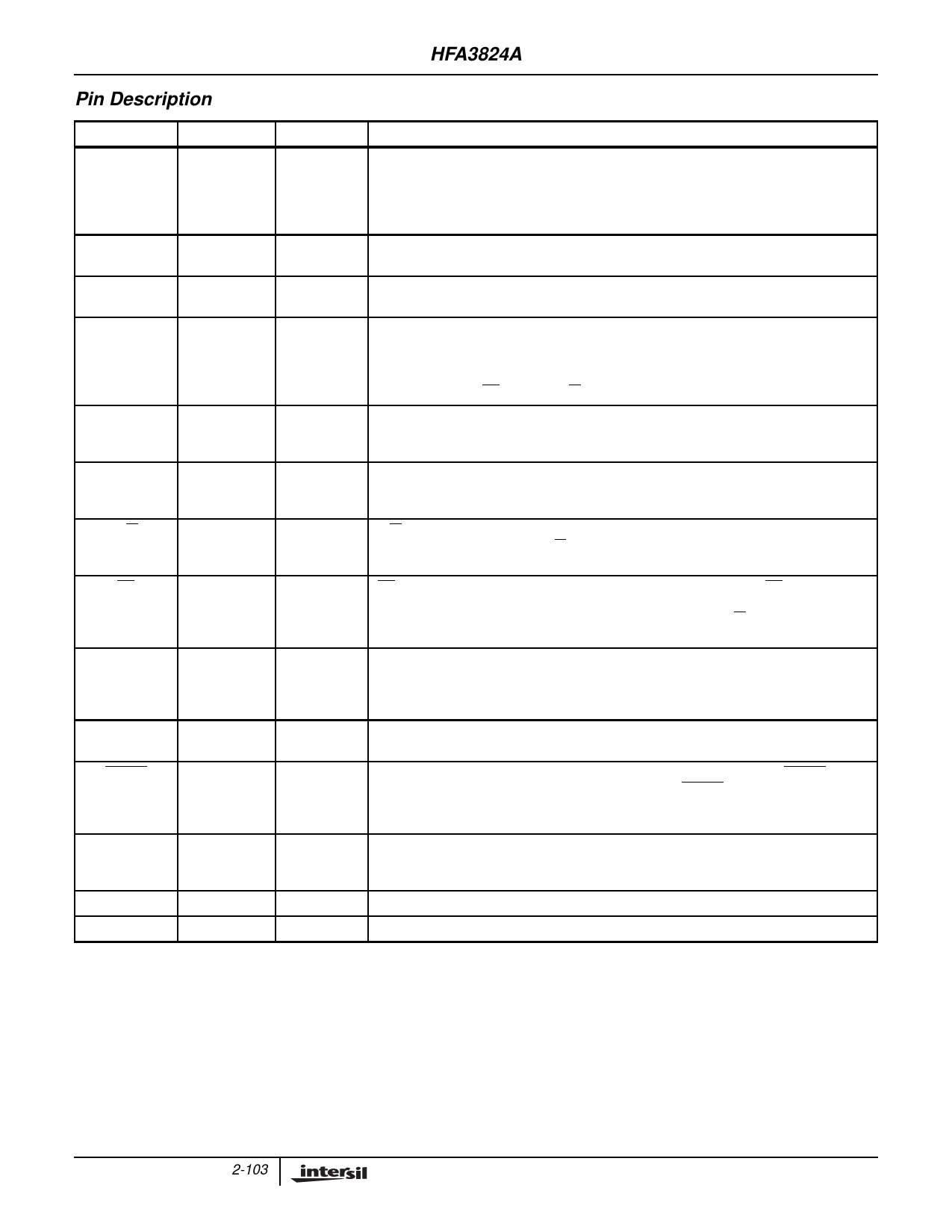
Pin Description (Continued)
NAME
MD_RDY
PIN
TYPE I/O
34
O
RX_PE
33
I
ANTSEL
27
O
SD
25
I/O
SCLK
24
I
AS
23
I
R/W
8
I
CS
9
I
TEST 0-7
37, 38, 39, 40,
I/O
43, 44, 45, 46
TEST_CK
1
O
RESET
28
I
MCLK
30
I
IOUT
48
O
QOUT
47
O
NOTE: Total of 48 pins; ALL pins are used.
DESCRIPTION
MD_RDY is an output signal to the network processor, indicating a data packet is ready to
be transferred to the processor. MD_RDY is an active high signal and it envelopes the data
transfer over the RXD serial bus. MD_RDY returns to its inactive state when there is no
more receiver data, when the programmable data length counter reaches its value or when
the link has been interrupted. MD_RDY remains inactive during preamble synchronization.
When active, receiver is configured to be operational, otherwise receiver is in standby
mode. This is an active high input signal. In standby, all A/D converters are disabled.
The antenna select signal changes state as the receiver switches from antenna to antenna
during the acquisition process in the antenna diversity mode.
SD is a serial bidirectional data bus which is used to transfer address and data to/from the
internal registers. The bit ordering of an 8-bit word is MSB first. The first 8 bits during trans-
fers indicate the register address immediately followed by 8 more bits representing the
data that needs to be written or read at that register. This pin goes to high impedance
(three-state) when CS is high or R/W is low.
SCLK is the clock for the SD serial bus. The data on SD is clocked at the rising edge. SCLK
is an input clock and it is asynchronous to the internal master clock (MCLK)The maximum
rate of this clock is 11MHz or one half the master clock frequency, whichever is lower.
AS is an address strobe used to envelope the Address or the data on SD.
Logic 1 = envelopes the address bits.
Logic 0 = envelopes the data bits.
R/W is an input to the HFA3824A used to change the direction of the SD bus when reading
or writing data on the SD bus. R/W must be set up prior to the rising edge of SCLK. A high
level indicates read while a low level is a write.
CS is a Chip select for the device to activate the serial control port. The CS doesn’t impact
any of the other interface ports and signals, i.e., the TX or RX ports and interface signals.
This is an active low signal. When inactive SD, SCLK, AS and R/W become “don’t care”
signals.
This is a data port that can be programmed to bring out internal signals or data for moni-
toring. These bits are primarily reserved by the manufacturer for testing. A further descrip-
tion of the test port is given at the appropriate section of this data sheet. The direction of
these pins are not established until programming of test registers is complete.
This is the clock that is used in conjunction with the data that is being output from the test
bus (TEST 0-7).
Master reset for device. When active TX and RX functions are disabled. If RESET is kept
low the HFA3824A goes into the power standby mode. RESET does not alter any of the
configuration register values nor it presets any of the registers into default values. Device
requires programming upon power-up.
Master Clock for device. The maximum frequency of this clock is 44MHz. This is used in-
ternally to generate all other internal necessary clocks and is divided by 1, 2, 4, or 8 for the
transceiver clocks.
TX Spread baseband I digital output data. Data is output at the programmed chip rate.
TX Spread baseband Q digital output data. Data is output at the programmed chip rate.
2-103
Share Link: 