HD74HC393 データシートの表示(PDF) - Renesas Electronics
部品番号
コンポーネント説明
一致するリスト
HD74HC393 Datasheet PDF : 9 Pages
| |||
HD74HC393
Switching Characteristics (CL = 50 pF, Input tr = tf = 6 ns)
Item
Maximum clock
frequency
Propagation delay
time
Pulse width
Removal time
Output rise/fall
time
Input capacitance
Symbol VCC (V)
fmax
2.0
4.5
6.0
tPLH
2.0
tPHL
4.5
6.0
tPLH
2.0
tPHL
4.5
6.0
tPLH
2.0
tPHL
4.5
6.0
tPLH
2.0
tPHL
4.5
6.0
tPHL
2.0
4.5
6.0
tw
2.0
4.5
6.0
th
2.0
4.5
6.0
tTLH
2.0
tTHL
4.5
6.0
Cin
—
Ta = 25°C
Min Typ Max
——
5
— — 25
— — 29
— — 120
— 16 24
— — 20
— — 185
— 20 37
— — 31
— — 220
— 24 44
— — 37
— — 260
— 28 52
— — 44
— — 150
— 21 30
— — 28
80 — —
16 — —
14 — —
50 — —
10 — —
9 ——
— — 75
— 5 15
— — 13
— 5 10
Ta = –40 to +85°C
Min
Max Unit
Test Conditions
—
4 MHz
—
20
—
24
—
150 ns Clock to QA
—
30
—
26
—
230 ns Clock to QB
—
46
—
39
—
275 ns Clock to QC
—
55
—
47
—
325 ns Clock to QD
—
65
—
55
—
190 ns Clear to QA, QB, QC, QD
—
38
—
33
100
—
ns Clock, clear
20
—
17
—
65
—
ns Clear to clock
13
—
11
—
—
95
ns
—
19
—
16
—
10 pF
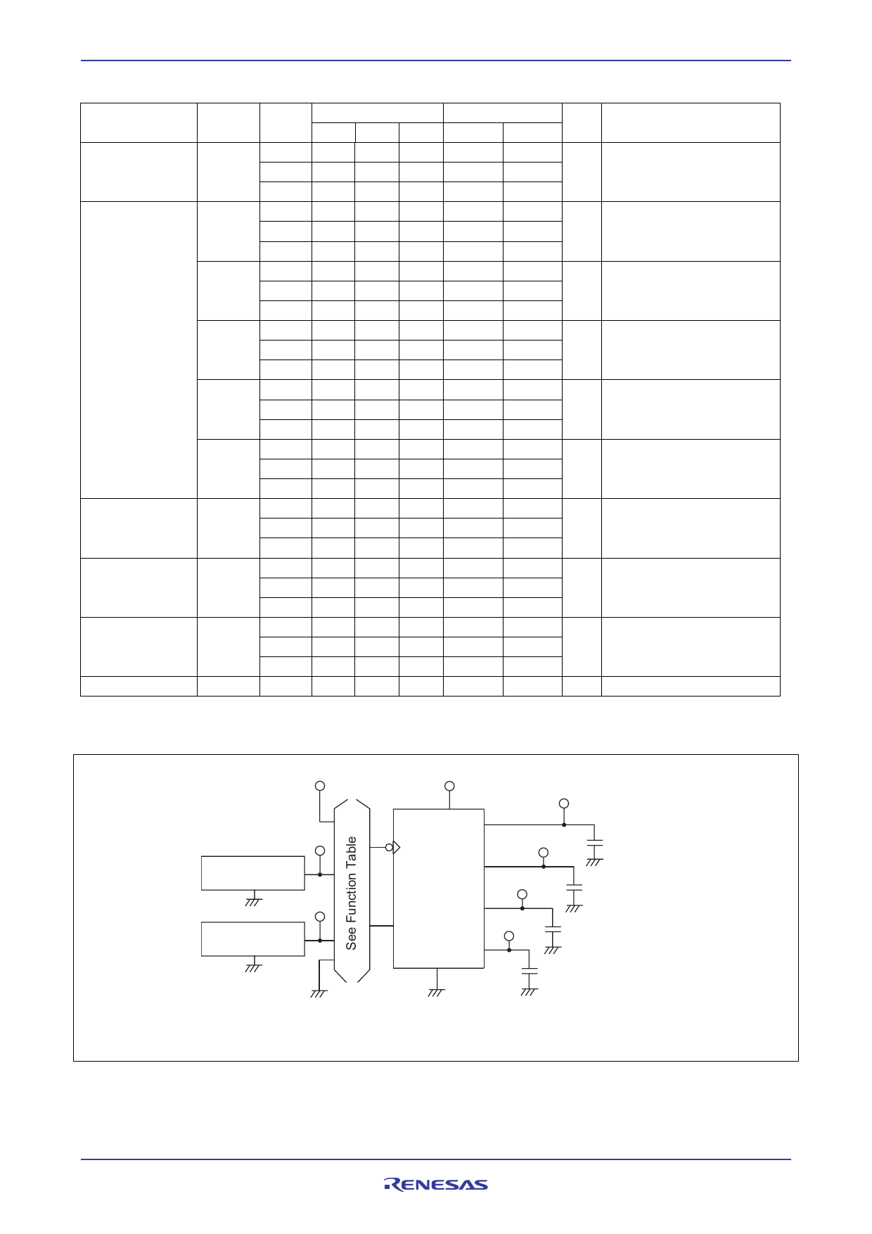
Test Circuit
VCC
Input
Pulse Generator
Zout = 50 Ω
Input
Pulse Generator
Zout = 50 Ω
VCC
Output
A
Clear
QA
Output
CL = 50 pF
QB
Output
QC
Output
QD
CL = 50 pF
CL = 50 pF
CL = 50 pF
Note : 1. CL includes probe and jig capacitance.
Rev.2.00 Mar 30, 2006 page 4 of 6
Share Link: 