RT9161-22CV データシートの表示(PDF) - Richtek Technology
部品番号
コンポーネント説明
一致するリスト
RT9161-22CV Datasheet PDF : 10 Pages
| |||
RT9161/A
Absolute Maximum Ratings
Input Voltage ----------------------------------------------------------------------------------------------------------- −0.3 to 14V
Operating Junction Temperature Range ------------------------------------------------------------------------ −40°C to 125°C
Storage Temperature Range --------------------------------------------------------------------------------------- −65°C to 150°C
Power Dissipation, PD @ TA = 25°C
SOT-89 ------------------------------------------------------------------------------------------------------------------ 0.5W
TO-92 -------------------------------------------------------------------------------------------------------------------- 0.6W
SOT-23 ------------------------------------------------------------------------------------------------------------------ 0.15W
Package Thermal Resistance
SOT-89, θJC ------------------------------------------------------------------------------------------------------------ 100°C /W
SOT-89, θJA ------------------------------------------------------------------------------------------- 300°C/W
SOT-223, θJC ----------------------------------------------------------------------------------------- 15°C/W
SOT-223, θJA ----------------------------------------------------------------------------------------- 60°C/W
TO-92, θJA --------------------------------------------------------------------------------------------------------------- 160° C/W
SOT-23, θJA ------------------------------------------------------------------------------------------------------------- 250° C/W
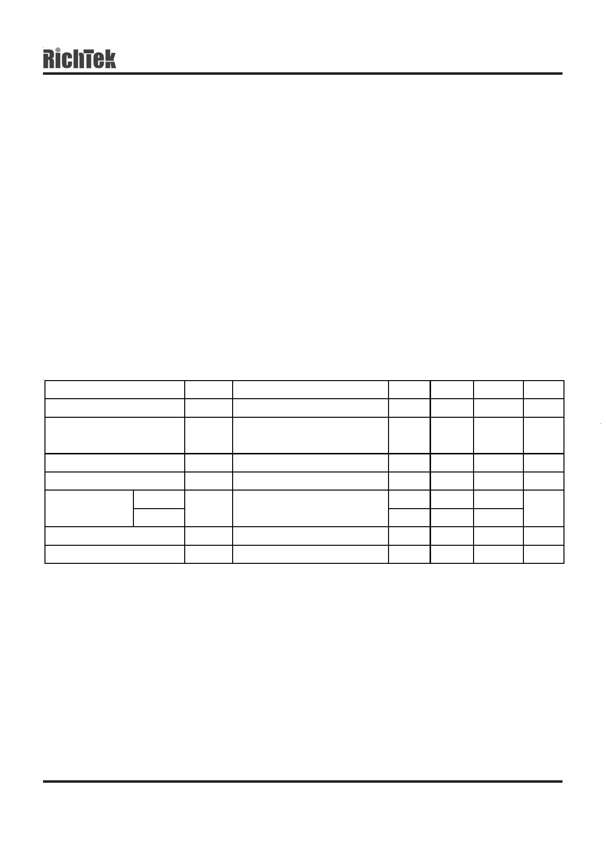
Electrical Characteristics
(TA = 25°C, CIN = 1µF, COUT = 10µF, unless otherwise specified.)
Parameter
Symbol
Test Conditions
Output Voltage Accuracy
∆VOUT IL = 1mA, VIN = 5V
Output Voltage Temperature
Coefficient
Min Typ
-2
--
--
50
Max Units
+2
%
150 PPM/°C
Line Regulation
∆VLINE
Load Regulation (1)
∆VLOAD
Current Limit (2)
RT9161
RT9161A ILIMIT
IL = 1mA, VIN= 4.5 ~ 12V
IL = 1mA ~ 300/500mA, VIN = 5V
VIN= 5V, VOUT = 0V
Dropout Voltage (3) (4)
Standby Current
VDROP IL = 300/500mA
ISTANDBY IL = 0, VIN = 12V
--
2
3
%VOUT
--
1
30/50 mV
350
580
--
mA
500
900
--
-- 450/750 600/1000 mV
--
110
180
µA
Note:
(1) Regulation is measured at constant junction temperature, using pulsed ON time.
(2) Current Limit is measured at constant junction temperature, using pulsed ON time.
(3) Dropout is measured at constant junction temperature, using pulsed ON time, and the criterion is VOUT inside target value
± 2%.
(4) Dropout test is skipped at the condition of VIN < 3V.
DS9161/A-23 April 2004
3
Share Link: 