EL7564 データシートの表示(PDF) - Intersil
部品番号
コンポーネント説明
一致するリスト
EL7564 Datasheet PDF : 17 Pages
| |||
EL7564
NMOS Power FETs and Drive Circuitry
The EL7564 integrates low on-resistance (30mΩ) NMOS
FETs to achieve high efficiency at 4A. In order to use an
NMOS switch for the high-side drive it is necessary to drive
the gate voltage above the source voltage (LX). This is
accomplished by bootstrapping the VHI pin above the LX
voltage with an external capacitor CVHI and internal switch
and diode. When the low-side switch is turned on and the
LX voltage is close to GND potential, capacitor CVHI is
charged through an internal switch to VDRV, typically 5V. At
the beginning of the next cycle the high-side switch turns
on and the LX pins begin to rise from GND to VIN potential.
As the LX pin rises the positive plate of capacitor CVHI
follows and eventually reaches a value of VDRV + VIN,
typically 10V, for VDRV = VIN = 5V. This voltage is then
level shifted and used to drive the gate of the high-side
FET, via the VHI pin. A value of 0.22µF for CVHI is
recommended.
Reference
A 1.5% temperature compensated bandgap reference is
integrated in the EL7564. The external VREF capacitor acts
as the dominant pole of the amplifier and can be increased
in size to maximize transient noise rejection. A value of
0.1µF is recommended.
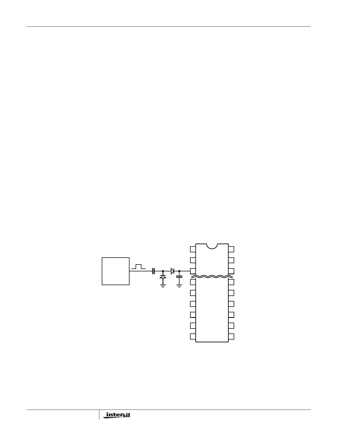
Oscillator
The system clock is generated by an internal relaxation
oscillator with a maximum duty-cycle of approximately 95%.
Operating frequency can be adjusted through COSC.
When external synchronization is required, always choose
COSC such that the free-running frequency is at least 20%
lower than that of the sync source to accommodate
component and temperature variations. Figure 21 shows a
typical connection.
Junction Temperature Sensor
An internal temperature sensor continuously monitors die
temperature. In the event that the die temperature exceeds
the thermal trip-point, the system is in a fault state and will
be shut down. The upper and low trip-points are set to 135°C
and 115°C respectively.
The VTJ pin is an accurate indication of the internal silicon
junction temperature (see performance curve.) The junction
temperature TJ (°C) can be determined from the following
relation:
TJ
=
75 + 1----.--2----–-----V----T----J--
0.00384
Where VTJ is the voltage at the VTJ pin in volts.
Power Good and Power On Reset
During power up the output regulator will be disabled until
VIN reaches a value of approximately 4V. About 500mV
hysteresis is present to eliminate noise-induced oscillations.
Under-voltage and over-voltage conditions on the regulator
output are detected through an internal window comparator.
A logic high on the PG output indicates that the regulated
output voltage is within about +10% of the nominal selected
EXTERNAL
OSCILLATOR
1
20
2
19
100pF BAT54S
3
18
390pF
5
16
6
EL7564
15
7
14
8
13
9
12
10
11
FIGURE 23. OSCILLATOR SYNCHRONIZATION
11
FN7297.3
May 9, 2005
Share Link: 