RF2617 データシートの表示(PDF) - RF Micro Devices
部品番号
コンポーネント説明
一致するリスト
RF2617 Datasheet PDF : 8 Pages
| |||
RF2617
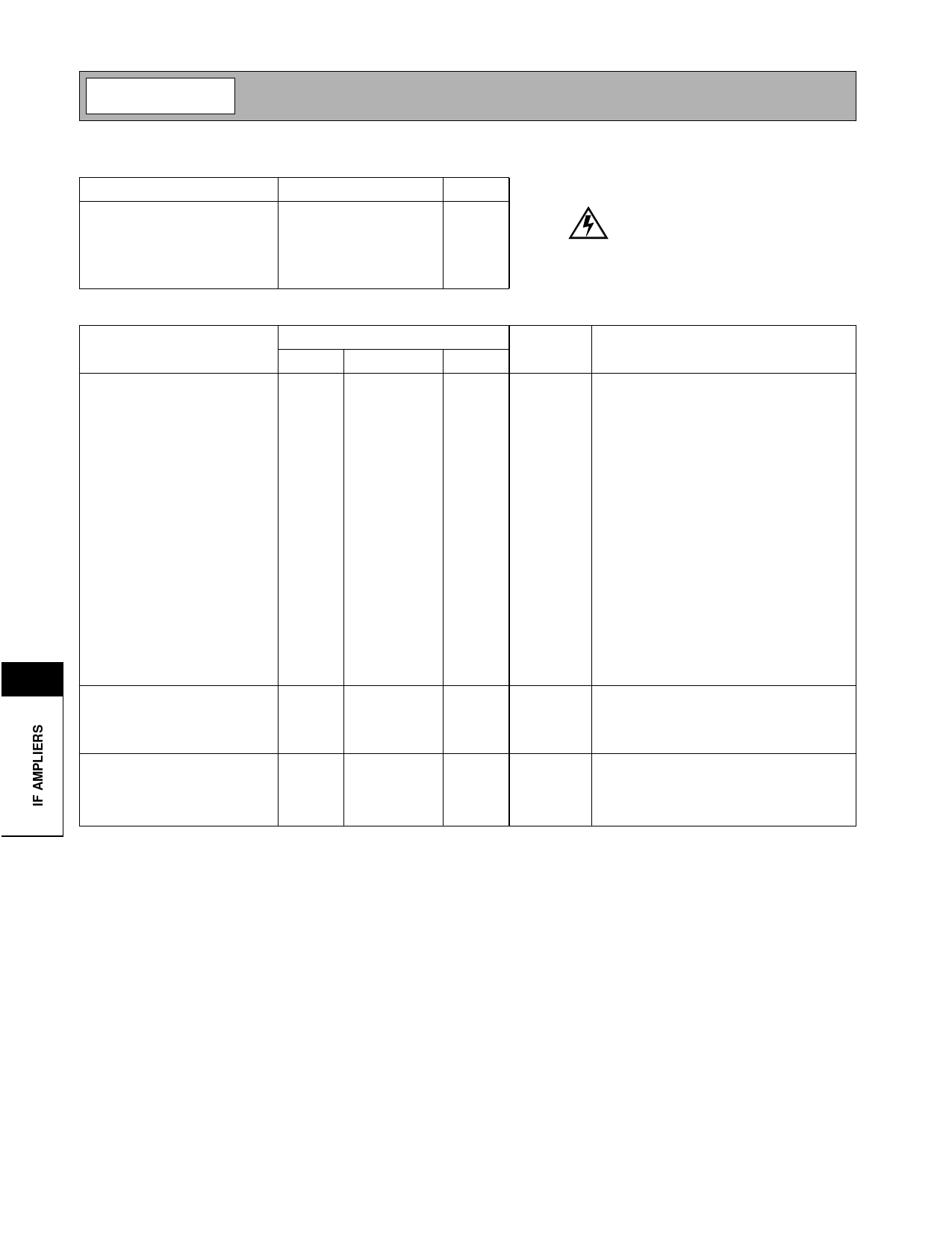
Absolute Maximum Ratings
Parameter
Supply Voltage
Control Voltage
Input RF Power
Operating Ambient Temperature
Storage Temperature
Value
-0.5 to +7.0
-0.5 to +5.0
+10
-40 to +85
-40 to +150
Unit
VDC
VDC
dBm
°C
°C
Parameter
Specification
Min.
Typ.
Max.
Overall
Frequency Range
12 to 285
CDMA Maximum Gain
+45
+48
CDMA Minimum Gain
-48
-45
FM Maximum Gain
+45
+49
FM Minimum Gain
-48
-45
Gain Slope
57
Gain Control Voltage Range
0 to 3
Gain Control Input Impedance
30
Noise Figure
5
8
10
Input IP3
Stability (Max VSWR)
IF Input
-44
-40
-4
-2
10:1
Input Impedance
1
Input Impedance
850
CDMA to FM Isolation
30
Power Supply
Voltage
2.7 to 3.3
Current Consumption
13
15
Current Consumption
14
16
Caution! ESD sensitive device.
RF Micro Devices believes the furnished information is correct and accurate
at the time of this printing. However, RF Micro Devices reserves the right to
make changes to its products without notice. RF Micro Devices does not
assume responsibility for the use of the described product(s).
Unit
MHz
dB
dB
dB
dB
dB/V
VDC
kΩ
dB
dBm
dBm
kΩ
Ω
dB
V
mA
mA
Condition
T=25°C, 85MHz, VCC=3.0V, ZS =500 Ω,
ZL=500Ω, 500Ω External CDMA Input Ter-
minating Resistor, 500Ω External Output
Terminating Resistor (Effective ZS=333Ω,
Effective ZL=250Ω) (See application sche-
matic).
VGC = 2.4 V
VGC = 0.3 V
VGC = 2.4 V
VGC = 0.3 V
Measured in 0.5V increments
Source impedance of 4.7kΩ
At maximum gain and 85MHz
At +40dB gain, referenced to 500Ω
At minimum gain, referenced to 500Ω
Spurious < -70 dBm
CDMA, differential
FM, single-ended
Minimum gain, VCC=3.0V
Maximum gain, VCC=3.0V
10-18
Rev B4 010717
Share Link: 