DG9408 データシートの表示(PDF) - Vishay Semiconductors
部品番号
コンポーネント説明
一致するリスト
DG9408 Datasheet PDF : 16 Pages
| |||
DG9408, DG9409
Vishay Siliconix
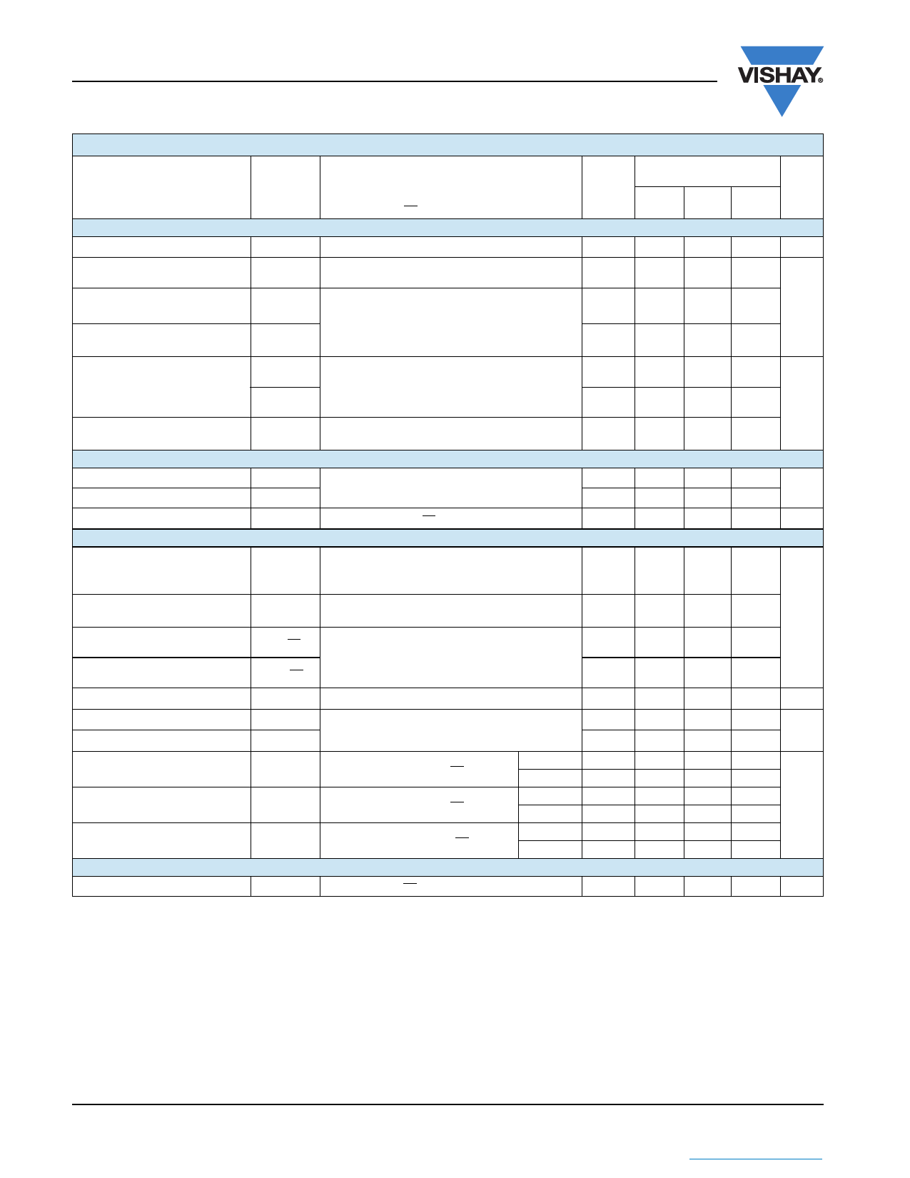
SPECIFICATIONS (Single Supply 3 V)
Parameter
Analog Switch
Symbol
Test Conditions
Unless Otherwise Specified
V+ = 3 V, ± 10 %, V- = 0 V
VEN = 0.4 V or 1.8 Vf
Limits
- 40 °C to 85 °C
Temp.b Min.c Typ.d Max.c Unit
Analog Signal Rangee
On-Resistance
VANALOG
Full
0
RON
V+ = 2.7 V, VD = 0.5 V or 2.2 V, IS = 5 mA
Room
Full
3
V
12 25.5
26.5
RON Match Between
Channelsg
On- Resistance Flatnessi
RON
RON
Flatness
V+ = 2.7 V, VD = 0.5 V or 2.2 V, IS = 5 mA
Room
Room
3.6
13
Switch Off Leakage Currenta
IS(off)
ID(off)
V+ = 3.3 V
VS = 2 V or 1 V, VD = 1 or 2 V
Room - 2
Full
- 15
Room - 2
Full
- 15
2
15
2
15
nA
Channel On Leakage Currenta
ID(on)
V+ = 3.3 V
Room - 2
VD = VS = 1 V or 2 V, sequence each switch on Full
- 15
2
15
Digital Control
Logic High Input Voltage
Logic Low Input Voltage
Input Currenta
Dynamic Characteristics
VINH
VINL
IIN
VAX = VEN = 1.8 V or 0.4 V
Full
1.8
Full
Full
-1
V
0.4
1
µA
Transition Time
tTRANS
VS1 = 1.5 V, VS8 = 0 V, (DG9408)
VS1b = 1.5 V, VS4b = 0 V, (DG9409)
see fig. 2
Room
Full
140 165
182
Break-Before-Make Time
tBBM
VS(all) = VDA = 1.5 V
see fig. 4
Room
2
63
Full
ns
Enable Turn-On Time
Enable Turn-Off Time
tON(EN)
tOFF(EN)
VAX = 0 V, VS1 = 1.5 V (DG9408)
VAX = 0 V, VS1b = 1.5 V (DG9409)
see fig. 3
Room
Full
Room
Full
140 162
178
76
97
104
Charge Injectione
Q
CL = 1 nF, RGEN = 0 , VGEN = 0 V
Room
7
pC
Off Isolatione, h
Crosstalke
OIRR
XTALK
f = 100 kHz, RL = 1 k
Room
- 81
dB
Room
- 85
Source Off Capacitancee
CS(off)
f = 1 MHz, VS = 0 V, VEN = 1.8 V
DG9408 Room
DG9409 Room
23
25
Drain Off Capacitancee
CD(off)
f = 1 MHz, VD = 0 V, VEN = 1.8 V
DG9408 Room
DG9409 Room
230
120
pF
Drain On Capacitancee
CD(on)
f = 1 MHz, VD = 0 V, VEN = 0 V
DG9408 Room
DG9409 Room
256
147
Power Supplies
Power Supply Current
I+
VEN = VA = 0 V or V+
Room
1
µA
Notes:
a. Leakage parameters are guaranteed by worst case test condition and not subject to production test.
b. Room = 25 °C, full = as determined by the operating temperature suffix.
c. The algebraic convention whereby the most negative value is a minimum and the most positive a maximum, is used in this data sheet.
d. Typical values are for DESIGN AID ONLY, not guaranteed nor subject to production testing.
e. Guaranteed by design, not subject to production test.
f. VIN = input voltage to perform proper function.
g. RDON = RDON Max - RDON Min.
h. Worst case isolation occurs on Channel 4 due to proximity to the drain pin.
i. RDON flatness is measured as the difference between the minimum and maximum measured values across a defined Analog signal.
Stresses beyond those listed under “Absolute Maximum Ratings” may cause permanent damage to the device. These are stress ratings only, and functional operation
of the device at these or any other conditions beyond those indicated in the operational sections of the specifications is not implied. Exposure to absolute maximum
rating conditions for extended periods may affect device reliability.
www.vishay.com
Document Number: 71870
6
S11-1229-Rev. C, 20-Jun-11
This document is subject to change without notice.
THE PRODUCTS DESCRIBED HEREIN AND THIS DOCUMENT ARE SUBJECT TO SPECIFIC DISCLAIMERS, SET FORTH AT www.vishay.com/doc?91000
Share Link: 