7C1001 データシートの表示(PDF) - Cypress Semiconductor
部品番号
コンポーネント説明
一致するリスト
7C1001 Datasheet PDF : 9 Pages
| |||
PRELIMINARY CCYY77CC11000012
Maximum Ratings
(Above which the useful life may be impaired. For user guidelines, Static Discharge Voltage . . . . . . . . . . . . . . . . . . . . . . . . >2001V
not tested.)
(per MILĆSTDĆ883, Method 3015)
Storage Temperature . . . . . . . . . . . . . . . . . . -65_C to +150_C
Ambient Temperature with
Power Applied . . . . . . . . . . . . . . . . . . . . . . . -55_C to +125_C
Supply Voltage on VCC Relative to GND[1] . -0.5V to +7.0V
DC Voltage Applied to Outputs
in High Z State[1] . . . . . . . . . . . . . . . . . . -0.5V to VCC + 0.5V
DC Input Voltage[1] . . . . . . . . . . . . . . . . -0.5V to VCC + 0.5V
LatchĆUp Current . . . . . . . . . . . . . . . . . . . . . . . . . . . >200 mA
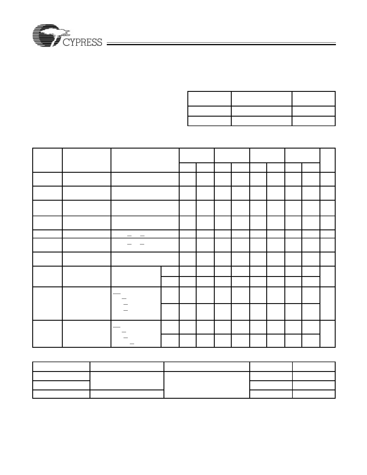
Operating Range
Range
TemApmerbaietunrte[2]
VCC
Commercial
0_C to + 70_C
5V ± 10%
Military
-55_C to + 125_C
5V ± 10%
Current into Outputs (LOW) . . . . . . . . . . . . . . . . . . . . . 20 mA
Electrical Characteristics Over the Operating Range[3]
77CC11000012--1122 77CC11000012--1155 77CC11000012--2200 77CC11000012--2255
Parameter Description
Test Conditions Min. Max. Min. Max. Min. Max. Min. Max. Unit
VOH
VOL
VIH
VIL
IIX
IOZ
IOS
ICC
ISB1
ISB2
Output HIGH
Voltage
Output LOW
Voltage
VCC = Min.,
IOH = -4.0 mA
2.4
2.4
2.4
2.4
V
VCC = Min., IOL = 8.0 mA
0.4
0.4
0.4
0.4 V
Input HIGH
Voltage
2.2 VCCā 2.2 VCCā 2.2 VCCā 2.2 VCCā V
+ā0.3
+ā0.3
+ā0.3
+ā0.3
Input LOW
Voltage[1]
-0.3 0.8 -0.3 0.8 -0.3 0.8 -0.3 0.8 V
InputLoadCurrent GND < VI < VCC
Output Leakage
Current
GND < VI < VCC,
Output Disabled
-1 +1 -1 +1 -1 +1 -1 +1 mA
-5 +5 -5 +5 -5 +5 -5 +5 mA
Output Short
Circuit Current[4]
VCC Operating
Supply Current
VCC = Max.,
VOUT = GND
VCC = Max.,
IOUT = 0 mA,
f = fMAX = 1/tRC
Com'l
Mil
-300
165
-300
155
165
-300
140
150
-300 mA
130 mA
140
Automatic CE
Max. VCC,
Com'l
50
40
30
30 mA
PowerĆDown
CE > VIH,
Current
VIN > VIH or
ĊĂTTL Inputs
VIN < VIL,
Mil
40
30
30
f = fMAX
Automatic CE
Max. VCC,
Com'l
2
2
2
2 mA
PowerĆDown
CE > VCC - 0.3V,
Current
ĊĂCMOS Inputs
VIN > VCC - 0.3V Mil
or VIN < 0.3V, f=0
2
2
2
Capacitance[5]
Parameter
Description
Test Conditions
Max.
Unit
CIN: Addresses
CIN: Controls
Input Capacitance
TA = 25_C, f = 1 MHz,
VCC = 5.0V
7
pF
10
pF
COUT
Output Capacitance
Notes:
1. VIL (min.) = -2.0V for pulse durations of less than 20 ns.
2. TA is the instant on" case temperature.
3. See the last page of this specification for Group A subgroup testing inĆ
formation.
10
pF
4. Not more than 1 output should be shorted at one time. Duration of the
short circuit should not exceed 30 seconds.
5. Tested initially and after any design or process changes that may affect
these parameters.
2
Share Link: 