CY7C026A-12AC データシートの表示(PDF) - Cypress Semiconductor
部品番号
コンポーネント説明
一致するリスト
CY7C026A-12AC Datasheet PDF : 18 Pages
| |||
CY7C026A
CY7C036A
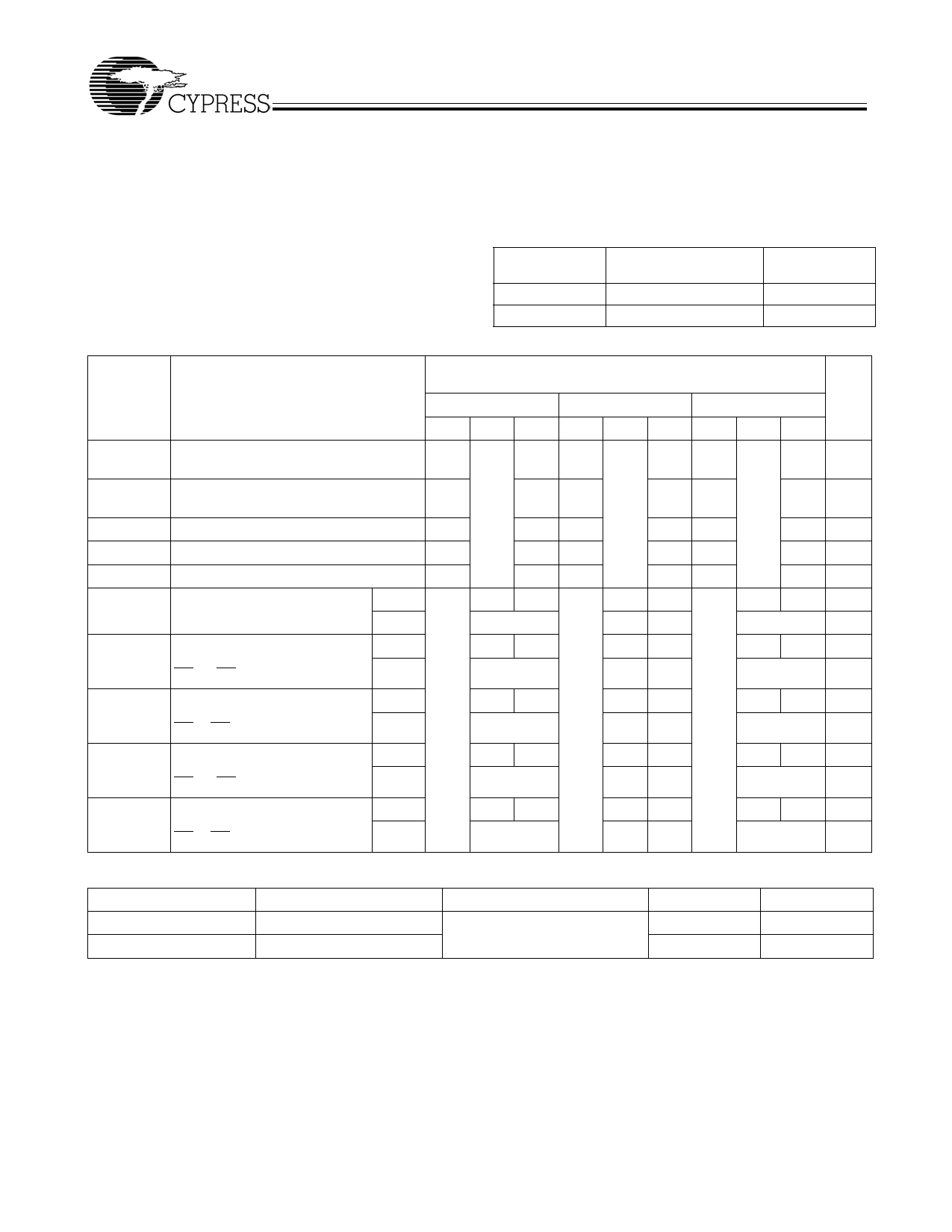
Maximum Ratings[5]
(Above which the useful life may be impaired. For user guide-
lines, not tested.)
Storage Temperature .................................–65°C to +150°C
Ambient Temperature with
Power Applied.............................................–55°C to +125°C
Supply Voltage to Ground Potential ............... –0.3V to +7.0V
DC Voltage Applied to Outputs
in High Z State ............................................... –0.5V to +7.0V
Electrical Characteristics Over the Operating Range
DC Input Voltage[6] ........................................–0.5V to + 7.0V
Output Current into Outputs (LOW)............................. 20 mA
Static Discharge Voltage........................................... >2001V
Latch-Up Current .................................................... >200 mA
Operating Range
Range
Commercial
Industrial
Ambient
Temperature
0°C to +70°C
–40°C to +85°C
VCC
5V ± 10%
5V ± 10%
Parameter
Description
VOH
Output HIGH Voltage
(VCC = Min., IOH = –4.0 mA)
VOL
Output LOW Voltage
(VCC = Min., IOH = +4.0 mA)
VIH
Input HIGH Voltage
VIL
Input LOW Voltage
IOZ
Output Leakage Current
ICC
Operating Current (VCC = Max., Com’l.
IOUT = 0 mA) Outputs Disabled Indust.
ISB1
Standby Current
Com’l.
(Both Ports TTL Level)
CEL & CER ≥ VIH, f = fMAX
Indust.
ISB2
Standby Current
Com’l.
(One Port TTL Level)
CEL | CER ≥ VIH, f = fMAX
Indust.
ISB3
Standby Current
Com’l.
(Both Ports CMOS Level)
CEL & CER ≥ VCC–0.2V, f = 0
Indust.
ISB4
Standby Current
Com’l.
(One Port CMOS Level)
CEL | CER ≥ VIH, f = fMAX[7]
Indust.
Capacitance[8]
Min.
2.4
2.2
–10
-12[1]
Typ. Max.
0.4
0.8
10
195 325
55 75
125 205
0.05 0.5
115 185
CY7C026A
CY7C036A
-15
Min. Typ. Max.
2.4
0.4
2.2
0.8
–10
10
190 285
215 305
50 70
65 95
120 180
135 205
0.05 0.5
0.05 0.5
110 160
125 175
Min.
2.4
2.2
–10
-20
Typ.
180
45
110
0.05
100
Max.
0.4
0.8
10
275
65
160
0.5
140
Unit
V
V
V
V
µA
mA
mA
mA
mA
mA
mA
mA
mA
mA
mA
Parameter
CIN
COUT
Description
Input Capacitance
Output Capacitance
Test Conditions
TA = 25°C, f = 1 MHz,
VCC = 5.0V
Max.
Unit
10
pF
10
pF
Notes:
5. The Voltage on any input or I/O pin cannot exceed the power pin during power-up.
6. Pulse width < 20 ns.
7. fMAX = 1/tRC = All inputs cycling at f = 1/tRC (except output enable). f = 0 means no address or control lines change. This applies only to inputs at CMOS level
standby ISB3.
8. Tested initially and after any design or process changes that may affect these parameters.
Document #: 38-06046 Rev. *C
Page 6 of 18
Share Link: 