CY7C026A-20AC(2000) データシートの表示(PDF) - Cypress Semiconductor
部品番号
コンポーネント説明
一致するリスト
CY7C026A-20AC Datasheet PDF : 17 Pages
| |||
CY7C026A
CY7C036A
Switching Characteristics Over the Operating Range[9]
CY7C026A
CY7C036A
-12[1]
-15
-20
Parameter
Description
Min. Max. Min. Max. Min. Max. Unit
READ CYCLE
tRC
Read Cycle Time
tAA
Address to Data Valid
tOHA
tACE[10]
Output Hold From Address Change
CE LOW to Data Valid
tDOE
tLZOE[11, 12, 13]
tHZOE[11, 12, 13]
tLZCE[11, 12, 13]
tHZCE[11, 12, 13]
tPU[13]
tPD[13]
tABE[10]
OE LOW to Data Valid
OE LOW to Low Z
OE HIGH to High Z
CE LOW to Low Z
CE HIGH to High Z
CE LOW to Power-Up
CE HIGH to Power-Down
Byte Enable Access Time
WRITE CYCLE
12
15
20
ns
12
15
20
ns
3
3
3
ns
12
15
20
ns
8
10
12
ns
3
3
3
ns
10
10
12
ns
3
3
3
ns
10
10
12
ns
0
0
0
ns
12
15
20
ns
12
15
20
ns
tWC
tSCE[10]
Write Cycle Time
CE LOW to Write End
12
15
20
ns
10
12
15
ns
tAW
Address Valid to Write End
10
12
15
ns
tHA
Address Hold From Write End
0
0
0
ns
tSA[10]
Address Set-Up to Write Start
0
0
0
ns
tPWE
Write Pulse Width
10
12
15
ns
tSD
tHD[15]
tHZWE[12, 13]
tLZWE[12, 13]
tWDD[14]
tDDD[14]
Data Set-Up to Write End
Data Hold From Write End
R/W LOW to High Z
R/W HIGH to Low Z
Write Pulse to Data Delay
Write Data Valid to Read Data Valid
10
10
15
ns
0
0
0
ns
10
10
12
ns
3
3
3
ns
25
30
45
ns
20
25
30
ns
Notes:
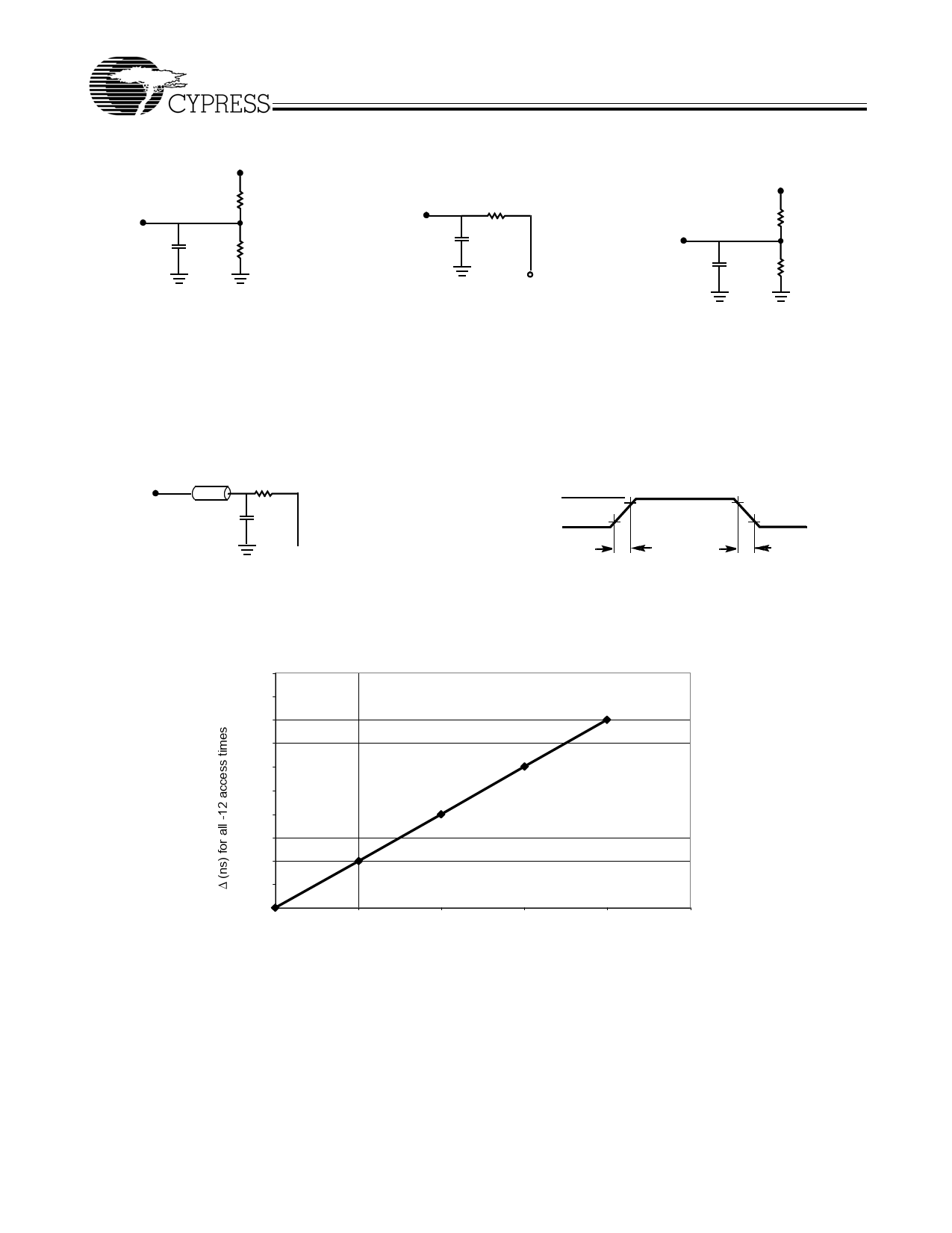
9. Test conditions assume signal transition time of 3 ns or less, timing reference levels of 1.5V, input pulse levels of 0 to 3.0V, and output loading of the specified
IOI/IOH and 30-pF load capacitance.
10. To access RAM, CE=L, UB=L, SEM=H. To access semaphore, CE=H and SEM=L. Either condition must be valid for the entire tSCE time.
11. At any given temperature and voltage condition for any given device, tHZCE is less than tLZCE and tHZOE is less than tLZOE.
12. Test conditions used are Load 3.
13. This parameter is guaranteed but not tested.
14. For information on port-to-port delay through RAM cells from writing port to reading port, refer to Read Timing with Busy waveform.
15. For 15 ns industrial parts tHD Min. is 0.5 ns.
7
Share Link: 