CY2308 データシートの表示(PDF) - Cypress Semiconductor
部品番号
コンポーネント説明
一致するリスト
CY2308 Datasheet PDF : 14 Pages
| |||
CY2308
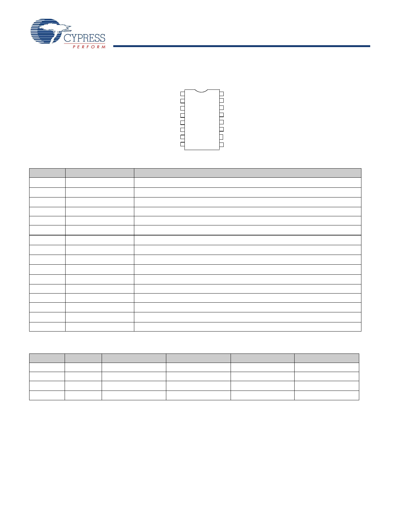
Pinouts
Figure 1. Pin Diagram - 16 Pin SOIC (Top view)
REF 1
CLKA1 2
CLKA2 3
VDD
4
GND 5
CLKB1 6
CLKB2 7
S2 8
16 FBK
15 CLKA4
14 CLKA3
13
VDD
12 GND
11 CLKB4
10 CLKB3
9 S1
Table 1. Pin Definitions - 16 Pin SOIC
Pin
Signal
1
REF[1]
2
CLKA1[2]
3
CLKA2[2]
4
VDD
5
GND
6
CLKB1[2]
7
CLKB2[2]
8
S2[3]
9
S1[3]
10
CLKB3[2]
11
CLKB4[2]
12
GND
13
VDD
14
CLKA3[2]
15
CLKA4[2]
16
FBK
Description
Input reference frequency, 5V tolerant input
Clock output, Bank A
Clock output, Bank A
3.3V supply
Ground
Clock output, Bank B
Clock output, Bank B
Select input, bit 2
Select input, bit 1
Clock output, Bank B
Clock output, Bank B
Ground
3.3V supply
Clock output, Bank A
Clock output, Bank A
PLL feedback input
Select Input Decoding
S2
S1
CLOCK A1–A4
0
0
Tri-State
0
1
Driven
1
0
Driven[4]
1
1
Driven
CLOCK B1–B4
Tri-State
Tri-State
Driven[4]
Driven
Output Source
PLL
PLL
Reference
PLL
PLL Shutdown
Y
N
Y
N
Notes
1. Weak pull down.
2. Weak pull down on all outputs.
3. Weak pull ups on these inputs.
4. Outputs inverted on 2308–2 and 2308–3 in bypass mode, S2 = 1 and S1 = 0.
Document Number: 38-07146 Rev. *F
Page 2 of 14
[+] Feedback
Share Link: 