CM200DY-34A データシートの表示(PDF) - Mitsumi
部品番号
コンポーネント説明
一致するリスト
CM200DY-34A Datasheet PDF : 5 Pages
| |||
MITSUBISHI IGBT MODULES
CM200DY-34A
HIGH POWER SWITCHING USE
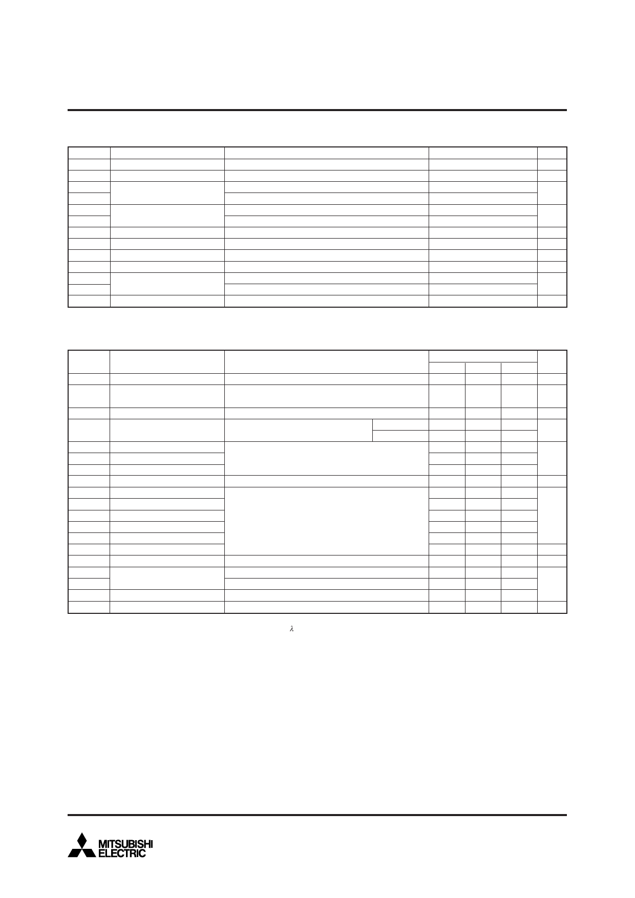
ABSOLUTE MAXIMUM RATINGS (Tj = 25°C, unless otherwise specified)
Symbol
VCES
VGES
IC
ICM
IE (Note 1)
IEM (Note 1)
PC (Note 3)
Tj
Tstg
Viso
—
—
—
Parameter
Collector-emitter voltage
Gate-emitter voltage
Collector current
Emitter current
Maximum collector dissipation
Junction temperature
Storage temperature
Isolation voltage
Torque strength
Weight
G-E Short
C-E Short
DC, TC = 109°C*1
Pulse
Operation
Pulse
TC = 25°C*1
Conditions
(Note 2)
(Note 2)
(Note 2)
(Note 2)
Terminals to base plate, f = 60Hz, AC 1 minute
Main terminals M6 screw
Mounting M6 screw
Typical value
Ratings
1700
±20
200
400
200
400
1980
–40 ~ +150
–40 ~ +125
3500
3.5 ~ 4.5
3.5 ~ 4.5
400
Unit
V
V
A
A
W
°C
°C
Vrms
N•m
g
ELECTRICAL CHARACTERISTICS (Tj = 25°C, unless otherwise specified)
Symbol
Parameter
Test conditions
Min.
ICES
Collector cutoff current
VCE = VCES, VGE = 0V
—
Gate-emitter threshold
VGE(th)
voltage
IC = 20mA, VCE = 10V
5.5
IGES
Gate leakage current
±VGE = VGES, VCE = 0V
—
VCE(sat)
Collector to emitter saturation
voltage
IC = 200A, VGE = 15V
Tj = 25°C
—
Tj = 125°C
—
Cies
Input capacitance
—
Coes
Output capacitance
VCE = 10V
—
Cres
Reverse transfer capacitance VGE = 0V
—
QG
Total gate charge
VCC = 1000V, IC = 200A, VGE = 15V
—
td(on)
Turn-on delay time
—
tr
Turn-on rise time
VCC = 1000V, IC = 200A
—
td(off)
Turn-off delay time
VGE = ±15V
—
tf
Turn-off fall time
RG = 2.4Ω, Inductive load
—
trr (Note 1) Reverse recovery time
IE = 200A
—
Qrr (Note 1) Reverse recovery charge
—
VEC(Note 1) Emitter-collector voltage
IE = 200A, VGE = 0V
—
Rth(j-c)Q
Rth(j-c)R
Thermal resistance
IGBT part (1/2 module)*1
FWDi part (1/2 module)*1
—
—
Rth(c-f)
Contact thermal resistance
Case to heat sink, Thermal compound applied (1/2 module)*1,*2
—
RG
External gate resistance
2.4
Limits
Typ.
—
7.0
—
2.2
2.45
—
—
—
1330
—
—
—
—
—
20
—
—
—
0.02
—
*1 : Case temperature (TC), heat sink temperature (Tf) measured point is just under the chips.
*2 : Typical value is measured by using thermally conductive grease of λ = 0.9[W/(m • K)].
Note 1. IE, IEM, VEC, trr & Qrr represent characteristics of the anti-parallel, emitter-collector free-wheel diode (FWDi).
2. Pulse width and repetition rate should be such that the device junction temperature (Tj) does not exceed Tjmax rating.
3. Junction temperature (Tj) should not increase beyond 150°C.
4. Pulse width and repetition rate should be such as to cause negligible temperature rise.
Max.
1
8.5
2.0
2.8
—
49.4
5.6
1.06
—
550
190
750
350
450
—
3.0
0.063
0.11
—
24
Unit
mA
V
µA
V
nF
nC
ns
µC
V
K/W
Ω
Feb. 2009
2
Share Link: 