CA3256 データシートの表示(PDF) - Harris Semiconductor
部品番号
コンポーネント説明
一致するリスト
CA3256 Datasheet PDF : 11 Pages
| |||
CA3256
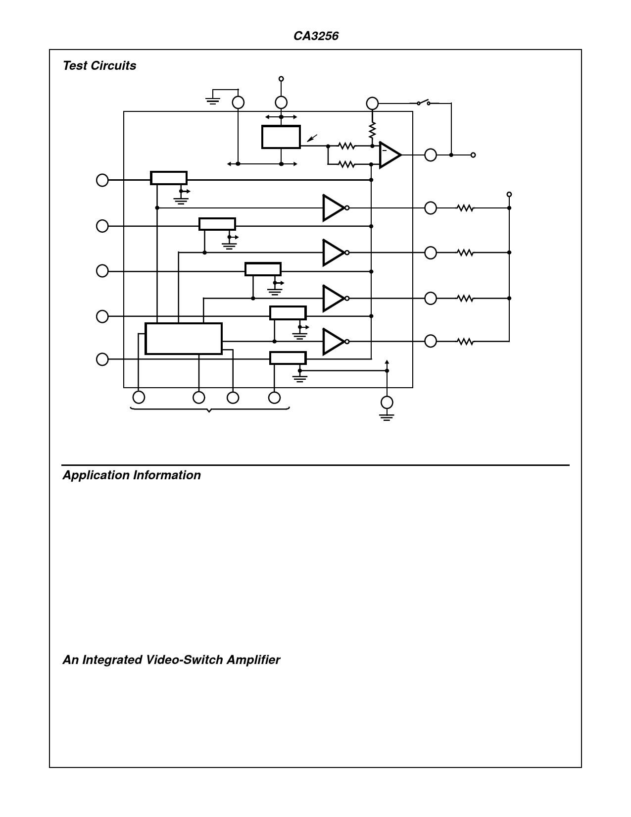
Test Circuits
IN 1
15
IN 2
17
IN 3
1
IN 4
3
IN/OUT 5
13
V-
V+ +12 V
5
14
FEEDBACK
8
FEEDBACK
SWITCH
TG-1
TG-2
LLC ENABLE
AND CHAN 1-4
SELECT
BIAS
REG
VBIAS
(V- +5V)
10K
10K
1
1K
+
OUTPUT
AMP
AMP
OUT
9
12
1.1K
2
TG-3
3
TG-4
4
TG-5
1.1K
11
1.1K
10
1.1K
2
VLED
+12 V
6 ENABLE
16 A 18 B
7C
CONTROL INPUTS (CHANNEL SELECT)
4 GND
FIGURE 1. CA3256 TEST CIRCUIT (DIP PINOUT)
Application Information
CMOS analog switches are available in a wide variety of
forms, and have been known and used for some time. There
are a number of advantages to using the CMOS transmis-
sion gate as a switch:
• Ideal Suitability to Series Cascade Arrangements
• Simple Multiple Parallel Input Switching Arrangements
• No Bipolar Junctions and, Hence, No Offset
• Very Low Power Consumption
• Wide Signal-Swing Capability
• Fast Multiplexing and Video Switching
• Wide Bandwidth
• Low RON Channel Resistance
• Bidirectional Signal Handling
An Integrated Video-Switch Amplifier
Commonly, integrated video-switch amplifiers have been fabri-
cated in the bipolar technology using differential amplifiers in a
current-switching mode. In this form, two differential pairs are
needed for two input-signal sources. The handling of multiple
sources is very much more complex. The advantages of the
CMOS video-switch amplifier have already been noted. While
the bipolar video switch has high output drive and switching
speed as advantages, the price is high in voltage offset and cur-
rent drain. The integrated device solution that is offered here is
in the use of the BiMOS technology, where both the CMOS and
bipolar processes complement each other to provide CMOS
switching with bipolar amplifiers. The BiMOS process allows
several CMOS switches to be coupled to a bipolar drive-ampli-
fier in the same process to exploit the best of two technologies.
Other advantages are gained when the BiMOS process is
used for an IC video-switch amplifier design. The BiMOS
process calls for a P-substrate and, therefore, isolated N-epi-
taxial wells can be built for both N and P channel parts. The
boats provide for better isolation of the N and P channels.
The N and P wells in a transmission-gate cell can be
switched between source and rail; therefore, they have a
smaller body effect on both N and P devices, which results in
better gain linearity. Where desired, oxide capacitors are
available for bipolar amplifier compensation.
CA3256 Video-Switch Amplifier
The Block Diagram shows the functional diagram of the
CA3256, which consists of five MOS channels, each com-
prising a three-element T-switch. The output of the five
switches is made common and fed into the input of a bipolar
8-5
Share Link: 