IMIC9530CY データシートの表示(PDF) - Cypress Semiconductor
部品番号
コンポーネント説明
一致するリスト
IMIC9530CY Datasheet PDF : 11 Pages
| |||
C9530
CXINPCB
CXINDISC
XIN
CXINFTG
CXOUTPCB
CXOUTDISC
XOUT CXOUTFTG
Clock Generator
As an example and using this formula for this data sheet’s
device, a design that has no discrete loading capacitors
(CDISC) and each of the crystal device PCB traces has a
capacitance (CPCB) to ground of 4 pF (typical value) would
calculate as follows.
Therefore, to obtain output frequencies that are as close to this
data sheets specified values as possible, in this design
example, you should specify a parallel cut crystal that is
designed to work into a load of 20 pF.
CL =
=
=
=
(4 pF + 36 pF + 0 pF) x (4 pF + 36 pF + 0 pF)
(4 pF + 36 pF + 0 pF) x (4 pF + 36 pF + 0 pF)
40 x 40
40 x 40
1600
80
20 pF
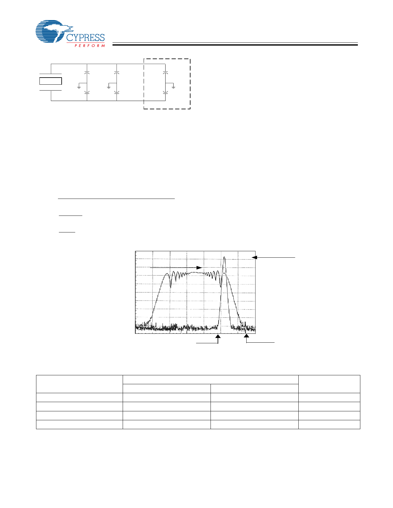
Spread Spectrum Clocking
Down Spread Description
Spread Spectrum is a modulation technique for distributing
clock period over a certain bandwidth (called Spread
Bandwidth). This technique allows the distribution of the
undesirable electromagnetic energy (EMI) over a wide range
of frequencies therefore reducing the average radiated energy
present at any frequency over a given time period. As the
spread is specified as a percentage of the resting (non-spread)
frequency value, it is effective at the fundamental and, to a
greater extent, at all it's harmonics.
In this device, Spread Spectrum is enabled externally through
pin 27 (SSCG#) or internally via SMBus Byte 0 Bit 0 and 6.
Spread spectrum is enabled externally when the SSCG# pin
is low. This pin has an internal device pull up resistor, which
causes its state to default to a high (Spread Spectrum
disabled) unless externally forced to a low. It may also be
enabled by programming SMBus Byte 0 Bit 0 LOW (to enable
SMBus control of the function) and then programming SMBus
Byte 0 Bit 6 LOW to set the feature active.
S p re a d o ff
S p re a d o n
C e n te r F re q u e n c y ,
S p re a d o n
C e n te r F re q u e n c y ,
S p re a d o ff
Figure 1. Spread Spectrum
Table 7. Spectrum Spreading Selection Table[7]
% of Frequency Spreading
Output Clock Frequency
SMBus Byte 0 Bit 5 = 0
SMBus Byte 0 Bit 5 = 1
Mode
33.3 MHz (XIN)
1.0% (–1.0% + 0%)
0.5% (–0.5% + 0%)
Down Spread
66.6 MHz (XIN*2)
1.0% (–1.0% + 0%)
0.5% (–0.5% + 0%)
Down Spread
100.0 MHz (XIN*3)
1.0% (–1.0% + 0%)
0.5% (–0.5% + 0%)
Down Spread
133.3 MHz (XIN*4)
1.0% (–1.0% + 0%)
0.5% (–0.5% + 0%)
Down Spread
Note:
7. When SSCG is enabled, the device will down spread the clock over a range that is 1% of its resting frequency. This means that for a 100-MHz output clock
frequency will sweep through a spectral range from 99 to 100 MHz.
Document #: 38-07033 Rev. *C
Page 6 of 11
Share Link: 