BSC072N025SG(2006) データシートの表示(PDF) - Infineon Technologies
部品番号
コンポーネント説明
一致するリスト
BSC072N025SG Datasheet PDF : 10 Pages
| |||
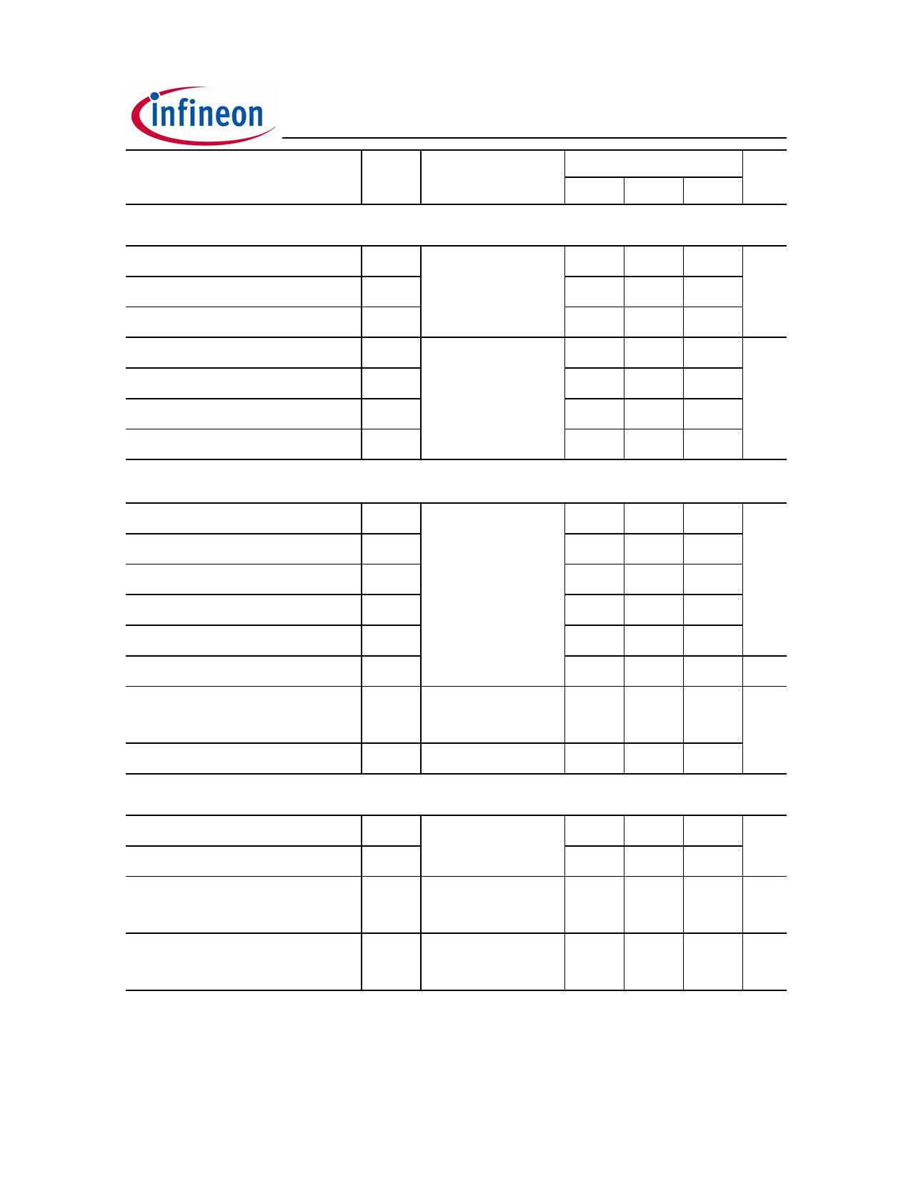
Parameter
Symbol Conditions
BSC072N025S G
min.
Values
typ.
Unit
max.
Dynamic characteristics
Input capacitance
Output capacitance
Reverse transfer capacitance
Turn-on delay time
Rise time
Turn-off delay time
Fall time
Gate Charge Characteristics4)
Gate to source charge
Gate charge at threshold
Gate to drain charge
Switching charge
Gate charge total
Gate plateau voltage
Gate charge total, sync. FET
Output charge
C iss
-
C oss
V GS=0 V, V DS=15 V,
f =1 MHz
-
Crss
-
t d(on)
-
tr
V DD=15 V, V GS=10 V,
-
t d(off)
I D=25 A, R G=2.7 Ω
-
tf
-
1680
643
80
5.3
4.8
21
3.8
2230 pF
855
120
7.9 ns
7.2
31
5.7
Q gs
-
5.6
7.4 nC
Q g(th)
-
2.7
3.6
Q gd
V DD=15 V, I D=25 A,
-
3.8
5.8
Q sw
V GS=0 to 5 V
-
6.7
9.6
Qg
-
13
18
V plateau
-
3.3
-V
Q g(sync)
V DS=0.1 V,
V GS=0 to 5 V
-
12
16 nC
Q oss
V DD=15 V, V GS=0 V
-
14
19
Reverse Diode
Diode continous forward current
Diode pulse current
Diode forward voltage
Reverse recovery charge
IS
I S,pulse
T C=25 °C
V SD
V GS=0 V, I F=40 A,
T j=25 °C
Q rr
V R=15 V, I F=I S,
di F/dt =400 A/µs
-
-
40 A
-
-
160
-
0.93
1.1 V
-
-
10 nC
4) See figure 16 for gate charge parameter definition
Rev. 0.94
page 3
2006-05-10
Share Link: 