BP5326 データシートの表示(PDF) - ROHM Semiconductor
部品番号
コンポーネント説明
一致するリスト
BP5326 Datasheet PDF : 4 Pages
| |||
Power Module
zPin descriptions
Pin No. Pin name
1
Co
2
VOUT
3
Vref
4, 7
GND
8
VCTL
9
VIN
Function
Output smoothing capacitor connection pin ; connect
a low-impedance capacitor with a recommended
capacitance of 47µF between this and GND.
Output pin.
Output voltage adjustment pin for contrast ; output
voltage is adjusted by connecting a resistor between
pins 2 and 3 or pins 3 and 4.
Ground pin.
Output ON/OFF control pin ; output starts when the
pin is HIGH level, and stops when the pin is LOW
or OPEN.
Input pin ; connect a low-impedance capacitor with
a recommended capacitance of 100µF between
this pin and GND.
BP5326
zElectrical characteristics (Unless otherwise noted, Ta=25°C, VCTL=5V, R1 to R2 resistors are disconnected)
Parameter
Symbol Min. Typ. Max. Unit
Conditions
Input voltage
VIN
4.5
5.0
5.5
V
−
Output current
IOUT
−
−
25
mA
−
Output voltage
VOUT1
28.0 29.5 31.0
V
VIN=4.5 to 5.5V, IOUT=0 to 25mA
Output voltage when OFF
VOUT2
−
−
0.3
V
VIN=4.5 to 5.5V, VCTL=0V
Ripple noise voltage
υ1
−
100
200
mVP-P VIN=5V, IOUT=20mA ∗
Efficiency
η
67
77
−
%
VIN=5V, IOUT=20mA
ON / OFF CTL voltage
when ON
VCTL
1.5
−
−
V
VIN=5V, Vo>28V
ON / OFF CTL voltage
when OFF
−
−
0.5
VCTL
V
VIN=5V, Vo<0.3V
(Alternatively, when OPEN)
ON / OFF CTL current
ICTL
−
−
500
µA
VIN=5V, VCTL=1.5V
Current consumption
when OFF
IOFF
−
−
50
µA
VIN=5V, VCTL=0V
∗ Measured with a band width of 20 MHz.
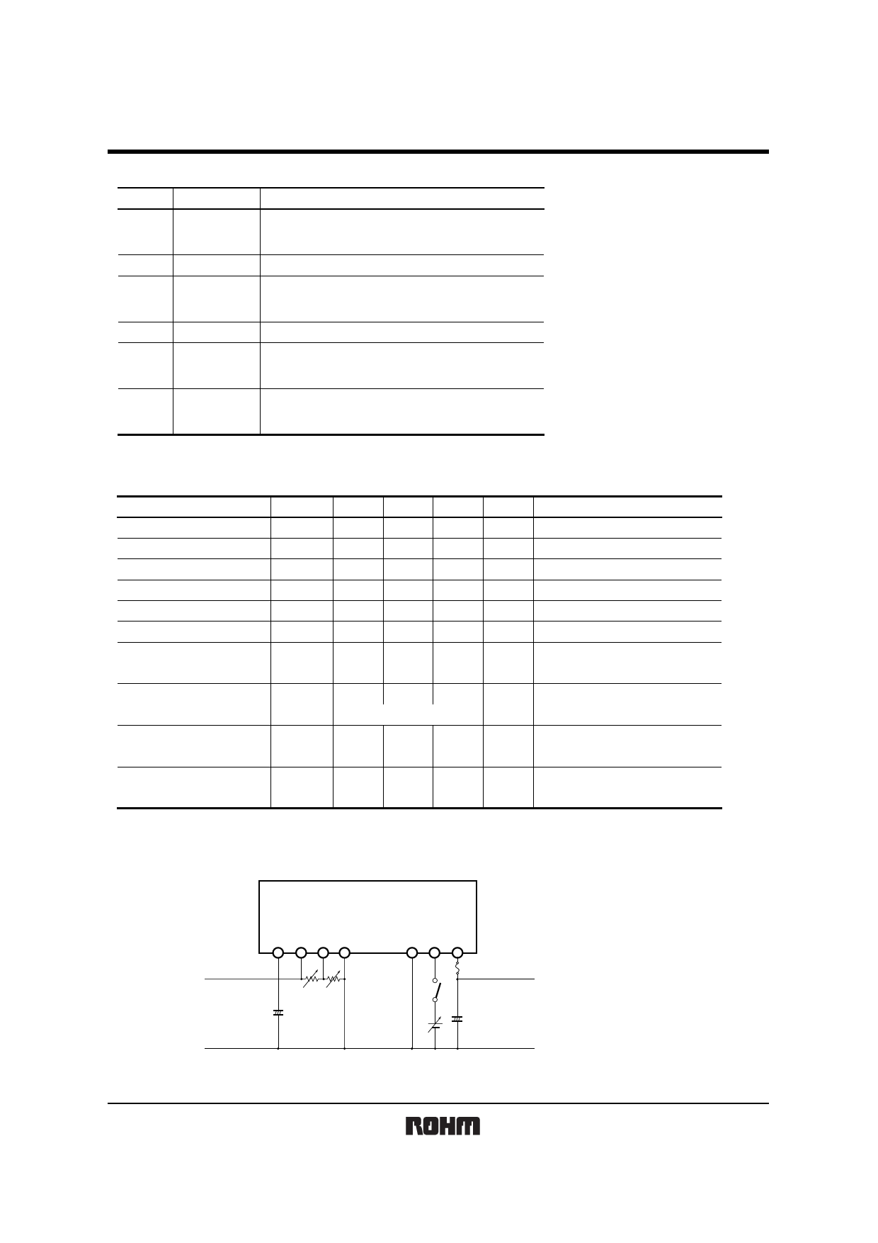
z Measurement circuit / Application example
VOUT
GND
BP5326
1 234
+
C2
R1
R2
78 9
Be sure to use
fuse for safety
VIN
VCTL
+
C1
Fig.1
GND
C1 : 100mF / 16V (Low impedance)
C2 : 47mF / 35V (Low impedance)
R1, 2 : Resistors for adjusting output voltage (Contrast adjustment)
Rev.A
2/3
Share Link: 