BP5302XA データシートの表示(PDF) - ROHM Semiconductor
部品番号
コンポーネント説明
一致するリスト
BP5302XA Datasheet PDF : 5 Pages
| |||
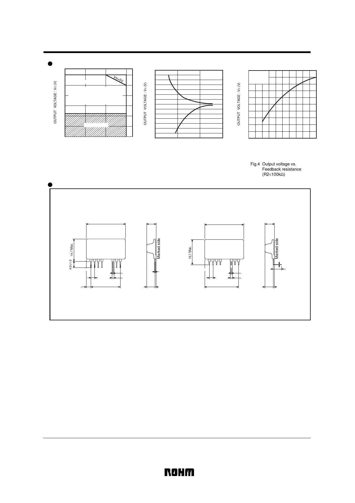
BP5302A / BP5302XA
Electrical characteristic curves
−30
−25
−20
−15
Ta=60°C
VIN=14V
VIN=5V
∗1. R1>50kΩ
R2>20kΩ
( ) R1 2pin − 3pin
R2 3pin − 4pin
∗2. Note that output voltage decreases with
increasing output current when the input
voltage VIN is low.
−10
−5
Unusable range
0
10
20
30
OUTPUT CURRENT : IO (mA)
Fig.2 Derating curve
External dimensions (Units : mm)
BP5302A
−31 R1 (R2= ∞)
−30
−29
−28
−27
−26
−25
−24
−23
−22
−21
−20
−19
−18 R2 (R1= ∞)
−17
100k
VIN=12V
Io=0mA
1M
10M
FEED BACK RESISTANCE : R1, R2 (Ω)
Fig.3 Output voltage vs.
Feedback resistance (R1, R2)
BP5302XA
−20
−19
VIN=12V
IO=0mA
−18
−17
−16
−15
−14
−13
−12
−11
10 20 30 40 50 60 70 80 90 100
FEED BACK RESISTANCE : R2 (kΩ)
Fig.4 Output voltage vs.
Feedback resistance
(R2<100kΩ)
26.0 Max.
6.0 Max.
26.0 Max.
6.0 Max.
Pin No.1 2 3 4 7 8 9
0.5±0.1
Pitch
2.54±0.2
1.4±0.2
2.9 Max.
2.54×8=20.32
4.6 Max.
0.27±0.05
1.4 Max.
SIP9
Pin No.1 2 3 4 7
Pitch
2.54±0.2
89
0.5±0.1
1.4±0.2
2.9 Max.
2.54×8=20.32
4.6 Max.
0.27±0.05
4.5 Min.
1.4 Max.
SIP9 (L forming)
3/4
Share Link: 